UM023 FMC230 User Manual
r1.11
UM023
www.4dsp.com
- 12 -
Card Type
Device
VCO Range
VCO
DAC Clock
FMC230
AD9517-1
2300MHz - 2650MHz
2457.60MHz
2457.60MHz
Table 3: FMC default clock configurations
Note
: Higher DAC clock frequencies (2850MHz for sampling up to 5700Msps) can be
achieved using external clock.
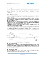
Figure 6: Loop filter design
4.10 Power supply
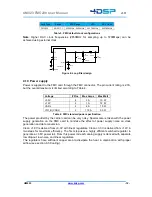
Power is supplied to the FMC card through the FMC connector. The pin current rating is 2.7A,
but the overall maximum is limited according to Table 4.
Voltage
# Pins
Max Amps
Max Watt
+3.3V
4
3 A
10 W
+12V
2
1 A
12 W
VADJ
4
4 A
10 W
VIO_B (VADJ)
2
1.15 A
2.3 W
Table 4: FMC standard power specification
The power provided by the carrier card can be very noisy. Special care is taken with the power
supply generation on the FMC card to minimize the effect of power supply noise on clock
generation and data conversion.
Clean +1.8V is derived from +3.3V with linear regulators. Clean +3.3V is derived from +12V in
two steps for maximum efficiency. The first step uses a highly efficient switched regulator to
generate a +3.8V power rail. From this power rail each analog supply is derived with separate
low dropout, low noise, and linear regulators.
The regulators have sufficient copper area to dissipate the heat in combination with proper
airflow (see section 6.3 Cooling).
220nF
Bypass
9
LF
8
CPRset
5.10k
CP Rset
46
/REFIN
47
CP
4
CLK
11
REFIN
48
Notes AD9517:
1. Consult manufacturer's data
s heet for full detail s
LD
2
AD9517-X
/CLK
12
Rset
44
Rset
4.12k
OUT 0
42
/OUT 0
41
OUT 1
39
/OUT 1
38
OUT 2
19
/OUT 2
20
OUT 3
22
/OUT 3
23
OUT 4
35
/OUT 4
34
OUT 5
33
/OUT 5
32
OUT 6
26
/OUT 6
27
OUT 7
28
/OUT 7
29
V Supply
Reference
30.7MHz
Gnd
V+
F out
R2
2.00k
C1
330pF
C2
4.70nF
R1
1.00k
C3
150pF


