background image

UM023 FMC230 User Manual  


r1.11 


UM023                   


www.4dsp.com


- 9 - 


4.4  Analog output channels 

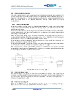
The  DAC  output  circuit  is  constructed  such  that  different  build  options  are  available.  The 
default configuration is a wideband balun ETC1-1-13 (MACOM; 4.5 to 3000MHz) as shown in 
Figure 4. This configuration is the recommended output circuit for mixed-mode operation of the 
DAC,  for  details  refer  to  the  AD9129  datasheet..  Please  contact  4DSP  for  custom 
configurations. 


4.4.1  Analog output phase 

While  not  intuitively  obvious  from  the  representative  schematic  below,  the  analog  output 
voltage tracks the data written to the DAC. The analog output signal at its maximum when the 
DAC is set to full scale. 

As shown in the schematic, the analog output connector X8 is directly connected to the DACs 
IOUTN (labeled DAC1_IN) signal thru the balun T4, this results in the output voltage tracking 
the voltage on the IOUTN pin.  

From  the  perspective  of  the  output  connector  and  IOUTN,  the  analog  output  is  formed  by  a 
voltage divider consisting of the high side pulled up to +1.8V by R89 and L13, and the low side 
pulled down to -1.5V by the DACs programmable current source. 

When  0x0000  is  written  to  the  DAC,  IOUTN  will  be  sourcing  its  maximum  current  thru  the 
pullups resulting in a negative output voltage. 

When the full scale value is written to the DAC, the current thru IOUTN and the pullups will be 
at its minimum resulting in the maximum positive voltage on the output. 

The  complementary  output  signal  IOUTP  performs  in  a  similar  manner  except  that  it  is  180 
degrees  out  of  phase  with  the  value  written  to the  DAC,  The IOUTP  and  IOUTN  signals  are 
combined by the transformer action of the balun T4. 


Figure 4: Wideband balun output option 

4.5  External trigger input 

An  external  trigger  is  available  on  the  front  panel  (MMCX  connector).  The  trigger  signal 
connects to a buffer (NB6N11S) before being sent to the carrier card. The buffer translates the 
external  LVTTL  signal  to  LVDS  and  connects  to  the  FMC  connector.  The  trigger  input  is 
terminated to ground with 4.7k

Ω.  


4.6  External clock input 

There  is  one  MMCX  clock  input  on  the  front  panel  that  can  serve  as  sampling  clock  input. 
Refer also to section 4.9 for more information about the clock tree. 

Summary of Contents for FMC230

Page 1: ...11 UM023 www 4dsp com 1 FMC230 User Manual 4DSP USA www 4dsp com forum This document is the property of 4DSP LLC and may not be copied nor communicated to a third party without the written permission...

Page 2: ...rect reference to analog input gain and over range in Chapter 2 1 4 2014 04 07 Revised some descriptions and fixed typos Changed external reference input characteristics 1 5 2014 05 30 Corrected analo...

Page 3: ...1 JTAG 7 4 3 Main characteristics 7 4 4 Analog output channels 9 4 4 1 Analog output phase 9 4 5 External trigger input 9 4 6 External clock input 9 4 7 External reference input 10 4 8 External clock...

Page 4: ...Low Voltage Differential Signaling MGT Multi Gigabit Transceiver MSB Most Significant Bit s PCB Printed Circuit Board PCI Peripheral Component Interconnect PCIe PCI Express PLL Phase Locked Loop PMC P...

Page 5: ...communication busses Furthermore the card is equipped with power supply and temperature monitoring and it offers several power down modes to switch off unused functions or protect the card from overh...

Page 6: ...ns The DAC devices use DDR LVDS signals mapped to the regular FMC pins Each channel has two 14 bit wide DDR LVDS busses Control signals operate in LVCMOS mode A VADJ range of 1 2V to 3 3V is supported...

Page 7: ...0 3P3VAUX 3P3V 12P0V VADJ JTAG see section 4 2 1 The bottom connector is not mounted by default 4 2 1 JTAG In a stacked environment the TDI pin will be decoupled from the TDO pin by the PRST_M2C_L sig...

Page 8: ...self biased to 1 5V refer to 4 7 Input impedance 5K Input range 0MHz to 250MHz External clock output Output Level 800mVp p into 50 typical LVCMOS output available as build option contact 4DSP Externa...

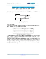
Page 9: ...g of the high side pulled up to 1 8V by R89 and L13 and the low side pulled down to 1 5V by the DACs programmable current source When 0x0000 is written to the DAC IOUTN will be sourcing its maximum cu...

Page 10: ...e clock generator specify VIL 0 8V and VIH 2 0V If the external reference source is DC coupled make sure that the VIL 0 8V and VIH 2 0V levels are met If the external reference source is AC coupled th...

Page 11: ...connector as a build option it can be connected to OUT7 OUT6 connects to the clock output on a MMCX connector 4 9 1 PLL design The PLL functionality of the AD9517 is used to operate from an internal s...

Page 12: ...tion on the FMC card to minimize the effect of power supply noise on clock generation and data conversion Clean 1 8V is derived from 3 3V with linear regulators Clean 3 3V is derived from 12V in two s...

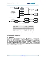
Page 13: ...y tree Power plane Typical Maximum VADJ 0 2A IVIO_B 3P3V 1 0A 1 1A 12P0V 0 2A 0 3A 3P3VAUX Operating 3P3VAUX Standby 0 1 mA 0 01 A 3 mA 1 A Table 5 Typical Maximum current drawn from FMC carrier card...

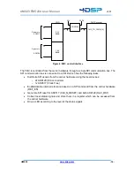
Page 14: ...ation bus is connected to a CPLD which has the following tasks Distribute SPI access from the carrier hardware along the local devices 2x AD9129 D A converters 1x AD9517 Clock Tree Enable disable inte...

Page 15: ...not connected SDIO is used bidirectional 3 wire SPI 5 2 SPI Programming The SPI programmable devices on the FMC can be accessed as described in their datasheet but each SPI communication cycle needs...

Page 16: ...ers A1 A0 8 bit pre selection P6 P5 P4 P3 P2 P1 P0 R W N1 N0 A4 A3 A2 A1 A0 8 bit instruction 8 bit register data D7 D6 D5 D4 D3 D3 D1 D0 N_CS SCLK SDIO P7 Figure 12 Write instruction to AD9129 regist...

Page 17: ...y operating the I2 C bus might interfere with the conversion process and result in signal distortion It is recommended to program the minimum and maximum limits in the monitoring devices and only read...

Page 18: ...defined in this document It is very likely that in these conditions the junction temperature of power consuming devices will exceed the operating conditions recommended by the device manufacturers mo...

Page 19: ...2 Connector Type MMCX Standard feature 1 SSMC 2 Reserved Standard Feature 1 Mil I 46058c Conformal Coating No Conformal Coating 1 Add Conformal Coating 2 Card Type 10 Warranty Hardware Software Firmw...

Page 20: ...DAC1_P0_DP05_P HB08_P F28 DAC1_P1_DP09_P LA05_N D12 DAC0_P0_DP02_N HA09_N E10 DAC1_P0_DP06_N HB09_N E28 DAC1_P1_DP08_N LA05_P D11 DAC0_P0_DP02_P HA09_P E9 DAC1_P0_DP06_P HB09_P E27 DAC1_P1_DP08_P LA06...

Page 21: ...C26 DAC0_P1_DP08_P LA28_N H32 DAC0_P1_DP12_N LA28_P H31 DAC0_P1_DP12_P LA29_N G31 DAC0_P1_DP11_N LA29_P G30 DAC0_P1_DP11_P LA30_N H35 DAC0_P1_DP13_N LA30_P H34 DAC0_P1_DP13_P LA31_N G34 FMC_TO_CPLD 1...

Page 22: ...rter DAC1_P0_N 13 0 DAC1_P1_P 13 0 D A 1 Input LVDS Data bus 1 going to the 2nd D A converter DAC1_P1_N 13 0 CLK_TO_FPGA_P I O Output LVDS Clock coming from the clock tree Typically used for debug and...

Page 23: ...sync AD9517 1 Assert CLK sync AD9517 Bit 6 5 Reserved Bit 7 EEPROM write enable Recommended to write 0 0x01 Control register 1 Bit 0 Reserved R O Bit 1 Reserved R O Bit 2 Reserved Bit 3 Reserved R O...

Reviews: