background image


Chapter 2 – Hardware Information 


21


3.5

” S

ub

co

mp
act

 Bo

ard


G

ENE

-HD05


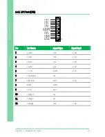
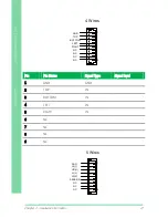
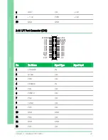
2.4.8  LPT Port Connector (CN8) 


N.C

N.C
N.C
N.C
N.C

GND
GND
GND
GND
GND
GND
GND
GND

N.C

DIO0
DIO1
DIO2
DIO3

N.C
N.C
N.C
N.C

DIO7
DIO6
DIO5
DIO4

STROBE#

1

2

25

26

1

2

25

26

AFD#

ERROR#

PRINT#

SLIN#

GND
GND
GND
GND
GND

GND

GND
GND

N.C

PD0
PD1
PD2
PD3
PD4
PD5
PD6
PD7

ACK#

BUSY

PE

SLCT

LPT Mode

DIO Mode

DIO7 

I/O 

+3.3V 

+3.3V 

PWR 

+3.3V 

10 

GND 

GND 


Pin 

Pin Name 

Signal Type 

Signal level 

1


STROBE# 

IN 


2


AFD# 

I/O 


3


PD0 

I/O 


4


ERROR# 

IN 


5


PD1 

I/O 


6


PRINT# 

I/O 


7


PD2 

I/O 


8


SLIN# 

I/O 


9


PD3 

I/O 


10


GND 

GND 


11


PD4 

I/O 


12


GND 

GND 


13


PD5 

I/O 


Summary of Contents for GENE-HD05

Page 1: ...Last Updated November 10 2015 GENE HD05 3 5 Subcompact Board User s Manual 4th Ed...

Page 2: ...in this manual is intended to be accurate and reliable However the original manufacturer assumes no responsibility for its use or for any infringements upon the rights of third parties that may resul...

Page 3: ...owners Microsoft Windows is a registered trademark of Microsoft Corp AMD is trademark of Advanced Micro Devices ITE is a trademark of Integrated Technology Express Inc IBM PC AT PS 2 and VGA are trade...

Page 4: ...ing up your product please make sure the following items have been shipped Item Quantity GENE HD05 1 Product DVD with User s Manual in pdf and drivers 1 If any of these items are missing or damaged pl...

Page 5: ...detailed descriptions and explanations on the product s hardware and software features if any its specifications dimensions jumper connector settings definitions and driver installation instructions i...

Page 6: ...ransient over voltage 7 Always disconnect this device from any AC supply before cleaning 8 While cleaning use a damp cloth instead of liquid or spray detergents 9 Make sure the device is installed nea...

Page 7: ...sion to the device iii Exposure to moisture iv Device is not working as expected or in a manner as described in this manual v The device is dropped or damaged vi Any obvious signs of damage displayed...

Page 8: ...plosion if the battery is incorrectly replaced Replace only with the same or equivalent type recommended by the manufacturer Dispose of used batteries according to the manufacturer s instructions and...

Page 9: ...Preface IX 3 5 Subcompact Board GENE HD05 China RoHS Requirements CN AAEON Main Board Daughter Board Backplane Pb Hg Cd Cr VI PBB PBDE O SJ T 11363 2006 X SJ T 11363 2006...

Page 10: ...enyl Ethers PBDE PCB Other Components X O O O O Wires Connectors for External Connections X O O O O O O The quantity of poisonous or hazardous substances or elements found in each of the component s p...

Page 11: ...ess Up down Selection JP5 11 2 3 6 LVDS Operating VDD Selection JP6 11 2 3 7 LVDS Operating VDD Selection JP6 11 2 3 7 LVDS Backlight Lightness Control Mode Selection JP7 12 2 3 8 LVDS Backlight Inver...

Page 12: ...CN20 29 2 4 21 5V Output for SATA HDD Connector CN21 30 2 4 22 5V Output for SATA HDD Connector CN22 30 2 4 23 LVDS Port Connector CN23 31 2 4 24 COM Port 1 D SUB 9 Connector CN24 32 2 4 25 Realtek L...

Page 13: ...ation 56 3 4 5 3 F81866 Super IO Configuration Serial Port 3 Configuration 58 3 4 5 4 F81866 Super IO Configuration Serial Port 4 Configuration 59 3 4 5 5 F81866 Super IO Configuration Parallel Port C...

Page 14: ...r Initial Program 80 Appendix B I O Information 82 B 1 I O Address Map 83 B 2 First MB Memory Address Map 85 B 3 IRQ Mapping Chart 86 B 4 DMA Channel Assignments 87 Appendix C Mating Connectors 88 C 1...

Page 15: ...3 5 Subcompact Board GENE HD05 Chapter 1 Chapter 1 Product Specifications...

Page 16: ...Ethernet 10 100 1000Base TX Realtek 8111E RJ 45 x 2 BIOS AMI Plug Play BIOS Wake On LAN Yes Watchdog Timer Generates a time out system reset H W Status Monitoring Supports power supply voltages fan s...

Page 17: ...up to 2560 x 1600 18W CRT 1920 x 1200 T40E T40R 6 5W 5 5W HDMI up to 1920 x 1200 Dual channel LVDS up to 1920 x 1200 LCD Interface 18 24 bit dual single channel LVDS Display Combination Simultaneous...

Page 18: ...3 5 Subcompact Board GENE HD05 Chapter 2 Chapter 2 Hardware Information...

Page 19: ...Chapter 2 Hardware Information 5 3 5 Subcompact Board GENE HD05 2 1 Dimensions Component Side Component Side Component Side...

Page 20: ...Chapter 2 Hardware Information 6 3 5 Subcompact Board GENE HD05 Solder Side Solder Side...

Page 21: ...Chapter 2 Hardware Information 7 3 5 Subcompact Board GENE HD05 2 2 Jumpers and Connectors Component Side Component Side Component Side...

Page 22: ...Chapter 2 Hardware Information 8 3 5 Subcompact Board GENE HD05 Solder Side Solder Side...

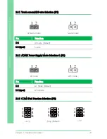
Page 23: ...pplication Label Function JP1 Touch Screen 4 5 8 wire Mode Selection JP2 AT ATX Power Supply Mode Selection 1 JP3 COM2 Pin8 Function Selection JP4 Clear CMOS Jumper JP5 LVDS Backlight Lightness Up Dow...

Page 24: ...tion JP1 4 8 wire mode 5 wire mode Pin 2BFunction 1 2 4 8 wire Default 1 2 open 5 wire 2 3 2 AT ATX Power Supply Mode Selection 1 JP2 AT mode ATX mode Pin Function 1 2 AT Mode Default 1 2 open ATX Mod...

Page 25: ...ghtness Up down Selection JP5 Lightness Up Lightness Down Note Up Down Selection is Push Button type interface do not use for Jumper Header and is only for PWM type Backlight Control JP7 2 3 2 3 6 LVD...

Page 26: ...light Lightness Control Mode Selection JP7 VR Mode Default PWM Mode 2 3 8 LVDS Backlight Inverter VCC Selection JP8 12 V 5 V Default 2 3 9 AT ATX Power Supply Mode Selection 2 JP9 At Mode Default ATX...

Page 27: ...e short JP9 set pin1 and pin2 to short If CN4 power input for 5VSB input is used please leave JP9 open set pin1 and pin2 to open Label Function CN1 LPC Port CN2 Touch Screen Connector CN3 CPU FAN CN4...

Page 28: ...CN21 5V Output for SATA HDD CN22 LVDS Inverter Backlight Connector CN23 LVDS Port CN24 COM Port 1 D SUB 9 CN25 Realtek LAN RJ 45 Port 2 CN26 Realtek LAN RJ 45 Port 1 CN27 USB Ports 1 and 2 CN28 HDMI P...

Page 29: ...LAD0 1 12 LAD1 LAD2 LAD3 LFRAME LRESET LDRQ0 LDRQ1 SERIRQ GND LCLK 3 3V Pin Pin Name Signal Type Signal level 1 LAD0 I O 3 3V 2 LAD1 I O 3 3V 3 LAD2 I O 3 3V 4 LAD3 I O 3 3V 5 3 3V PWR 3 3V 6 LFRAME I...

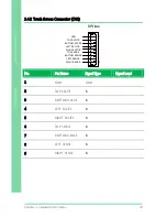
Page 30: ...GND 2 TOP EXCITE IN 3 BOTTOM EXCITE IN 4 LEFT EXCITE IN 5 RIGHT EXCITE IN 6 TOP SENSE IN 7 BOTTOM SENSE IN 8 LEFT SENSE IN 9 RIGHT SENSE IN GND 1 9 1 9 TOP EXCITE BOTTOM EXCITE LEFT EXCITE RIGHT EXCIT...

Page 31: ...E LEFT SENSE RIGHT SENSE GND TOP BOTTOM LEFT RIGHT NC NC NC NC GND UL Y UR H LL L LR X SENSE S NC NC NC 8 Wires 4 Wires 5 Wires 1 9 1 9 1 9 GND TOP BOTTOM LEFT RIGHT NC NC NC NC GND UL Y UR H LL L LR...

Page 32: ...set by JP1 2 4 3 CPU FAN Connector CN3 GND 1 2 3 FAN_POWER FAN_TAC 4 FAN_CTL Pin Pin Name Signal Type Signal level 1 GND GND 2 UL Y IN 3 UR H IN 4 LL L IN 5 LR X IN 6 SENSE S IN 7 NC 8 NC 9 NC Pin Pi...

Page 33: ...B Input Connector CN4 2 4 5 External 5VSB Input Connector CN5 2 4 6 Front Panel Connector CN6 5VSB GND PS_ON 1 2 3 12V GND 1 2 3 4 5 6 7 8 9 10 Pin Pin Name Signal Type Signal level 1 PS_ON OUT 5V 2 G...

Page 34: ...4 5 6 7 8 9 10 Pin Pin Name Signal Type Signal level 1 PWR_BTN 2 PWR_BTN 3 HDD_LED 4 HDD_LED 5 SPEAKER 6 SPEAKER 7 PWR_LED 8 PWR_LED 9 H W RESET 10 H W RESET Pin Pin Name Signal Type Signal level 1 DI...

Page 35: ...7 DIO6 DIO5 DIO4 STROBE 1 2 25 26 1 2 25 26 AFD ERROR PRINT SLIN GND GND GND GND GND GND GND GND N C PD0 PD1 PD2 PD3 PD4 PD5 PD6 PD7 ACK BUSY PE SLCT LPT Mode DIO Mode 8 DIO7 I O 3 3V 9 3 3V PWR 3 3V...

Page 36: ...HD05 2 4 9 COM Port 2 Connector CN9 1 2 3 4 5 6 7 8 9 14 GND GND 15 PD6 I O 16 GND GND 17 PD7 I O 18 GND GND 19 ACK IN 20 GND GND 21 BUSY IN 22 GND GND 23 PE IN 24 GND GND 25 SLCT IN 26 NC RS 232 Pin...

Page 37: ...CTS IN 7 DTR OUT 9V 8 RI 5V 12V IN PWR 5V 12V 9 GND GND RS 422 Pin Pin Name Signal Type Signal level 1 RS422_TX OUT 5V 2 NC 3 RS422_RX IN 4 NC 5 RS422_TX OUT 5V 6 NC 7 RS422_RX IN 8 NC 5V 12V PWR 5V...

Page 38: ...ing Default is RS 232 Pin 8 function can be set by Jumper 2 4 10 COM Port 3 Connector CN10 DCD DSR RX RTS TX CTS DTR RI GND 5 RS485_D I O 5V 6 NC 7 NC 8 NC 5V 12V PWR 5V 12V 9 GND GND Pin Pin Name Sig...

Page 39: ...Connector CN11 2 4 12 USB 2 0 Ports 7 Connector CN12 DCD DSR RX RTS TX CTS DTR RI GND Pin Pin Name Signal Type Signal level 1 DCD IN 2 DSR IN 3 RX IN 4 RTS OUT 9V 5 TX OUT 9V 6 CTS IN 7 DTR OUT 9V 8...

Page 40: ...rts 8 Connector CN13 2 4 14 USB 2 0 Ports 5 Connector CN14 3 USB7_D DIFF 4 GND GND 5 GND GND Pin Pin Name Signal Type Signal level 1 5VSB PWR 5V 2 USB8_D DIFF 3 USB8_D DIFF 4 GND GND 5 GND GND Pin Pin...

Page 41: ...2 0 Ports 6 Connector CN15 2 4 16 USB 2 0 Ports 3 Connector CN16 5 GND GND Pin Pin Name Signal Type Signal level 1 5VSB PWR 5V 2 USB6_D DIFF 3 USB6_D DIFF 4 GND GND 5 GND GND Pin Pin Name Signal Type...

Page 42: ...nector CN18 MIC_L 1 10 MIC_R LINE_L_IN LINE_R_IN LEFT_OUT RIGHT_OUT 5V_AUDIO GND_AUDIO GND_AUDIO GND_AUDIO Pin Pin Name Signal Type Signal level 1 5VSB PWR 5V 2 USB4_D DIFF 3 USB4_D DIFF 4 GND GND 5 G...

Page 43: ...2 4 20 SATA Port 1 Connector CN20 Pin 1 Pin 7 Pin 1 Pin 7 7 LEFT_OUT OUT 8 GND_AUDIO GND 9 RIGHT_OUT OUT 10 5V_AUDIO PWR 5V Pin Pin Name Signal Type Signal level 1 GND GND 2 SATA_TX DIFF 3 SATA_TX DIF...

Page 44: ...Output for SATA HDD Connector CN22 5V GND BLK_PWR 2 3 4 5 1 BKL_CONTROL GND GND BKL_ENABLE 2 SATA_TX DIFF 3 SATA_TX DIFF 4 GND GND 5 SATA_RX DIFF 6 SATA_RX DIFF 7 GND GND Pin Pin Name Signal Type Sig...

Page 45: ...can be set by JP7 2 4 23 LVDS Port Connector CN23 PIN 1 PIN 2 PIN 30 PIN 29 4 GND GND 5 BKL_ENABLE OUT 5V Pin Pin Name Signal Type Signal level 1 BKL_ENABLE OUT 2 BKL_CONTROL OUT 3 LCD_PWR PWR 3 3V 5...

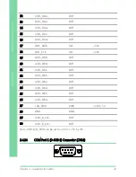
Page 46: ...r CN24 1 5 6 9 12 LVDS_DA1 DIFF 13 LVDS_DA2 DIFF 14 LVDS_DA2 DIFF 15 LVDS_DA3 DIFF 16 LVDS_DA3 DIFF 17 DDC_DATA I O 3 3V 18 DDC_CLK I O 3 3V 19 LVDS_DB0 DIFF 20 LVDS_DB0 DIFF 21 LVDS_DB1 DIFF 22 LVDS_...

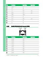
Page 47: ...ector CN25 1 ACT LINK LED SPEED LED 8 Pin Pin Name Signal Type Signal level 1 DCD IN 2 RX IN 3 TX OUT 9V 4 DTR OUT 9V 5 GND GND 6 DSR IN 7 RTS OUT 9V 8 CTS IN 9 RI IN Pin Pin Name Signal Type Signal l...

Page 48: ...Connector CN26 2 4 27 USB Port 1 and 2 Connector CN27 1 ACT LINK LED SPEED LED 8 Pin Pin Name Signal Type Signal level 1 MDI0 DIFF 2 MDI0 DIFF 3 MDI1 DIFF 4 MDI2 DIFF 5 MDI2 DIFF 6 MDI1 DIFF 7 MDI3 D...

Page 49: ...GND GND 5 5VSB PWR 5V 6 USB2_D DIFF 7 USB2_D DIFF 8 GND GND Pin Pin Name Signal Type Signal level 1 TMDS_Data2 DIFF 2 GND GND 3 TMDS_ Data2 DIFF 4 TMDS_ Data1 DIFF 5 GND GND 6 TMDS_ Data1 DIFF 7 TMDS...

Page 50: ...Connector CN29 2 4 30 VGA Port Connector CN30 KB_CLK KB_DATA 1 4 6 2 MS_DATA 5VSB GND MS_CLK 14 NC 15 SCL I O 3 3V 16 SDA I O 3 3V 17 GND 18 5V PWR 5V 19 HPLG_DETECT IN Pin Pin Name Signal Type Signal...

Page 51: ...2 Pin Pin Name Signal Type Signal level 1 RED OUT 2 GREEN OUT 3 BLUE OUT 4 NC 5 GND GND 6 RED_GND_RTN GND 7 GREEN_GND_RTN GND 8 BLUE_GND_RTN GND 9 5V PWR 5V 10 GND GND 11 NC 12 DDC_DATA I O 5V 13 HSYN...

Page 52: ...M1 Standard Specification 2 4 33 CFast Slot CFDA1 3 UIM_CLK IN 4 GND GND 5 UIM_VPP PWR 6 UIM_DATA I O Pin Pin Name Signal Type Signal level S1 GND GND S2 SATA_TX DIFF S3 SATA_TX DIFF S4 GND GND S5 SAT...

Page 53: ...C8 NC PC9 NC PC10 NC PC11 NC PC12 NC PC13 3 3V PWR 3 3V PC14 3 3V PWR 3 3V PC15 GND GND PC16 GND GND PC17 NC Pin Pin Name Signal Type Signal level 1 PCIE_WAKE IN 2 3 3VSB PWR 3 3V 3 NC 4 GND GND 5 NC...

Page 54: ...15 GND GND 16 UIM_VPP PWR 17 NC 18 GND GND 19 NC 20 W_DISABLE OUT 3 3V 21 GND GND 22 PCIE_RST OUT 3 3V 23 PCIE_RX DIFF 24 3 3VSB PWR 3 3V 25 PCIE_RX DIFF 26 GND GND 27 GND GND 28 1 5V PWR 1 5V 29 GND...

Page 55: ...Information 41 3 5 Subcompact Board GENE HD05 37 GND GND 38 USB_D DIFF 39 3 3VSB PWR 3 3V 40 GND GND 41 3 3VSB PWR 3 3V 42 NC 43 GND GND 44 NC 45 NC 46 NC 47 NC 48 1 5V PWR 1 5V 49 NC 50 GND GND 51 NC...

Page 56: ...3 5 Subcompact Board GENE HD05 Chapter 3 Chapter 3 AMI BIOS Setup...

Page 57: ...heck the current system configuration against the values stored in the CMOS memory If they do not match an error message will be outputted in which case you will need to run the BIOS setup program to...

Page 58: ...hen the power is turned off To enter BIOS Setup press Del or F2 immediately while your computer is powering up The function for each interface can be found below Main Date and time can be set here Pre...

Page 59: ...5 Subcompact Board GENE HD05 3 3 Setup submenu Main Options summary default setting System Date Day MM DD YYYY Change the month year and century The Day is changed automatically System Time HH MM SS C...

Page 60: ...vanced Options summary default setting ACPI Settings System ACPI Parameters CPU Configuration CPU Configuration Parameters SATA Configuration SATA Device Options Settings USB Configuration USB Configu...

Page 61: ...Chapter 3 AMI BIOS Setup 47 3 5 Subcompact Board GENE HD05 F81866 H W Monitor Monitor hardware status...

Page 62: ...48 3 5 Subcompact Board GENE HD05 3 4 1 Advanced ACPI Settings Options summary default setting ACPI Sleep State S3 Suspend to RAM Select the highest ACPI sleep state the system will enter when the SU...

Page 63: ...Chapter 3 AMI BIOS Setup 49 3 5 Subcompact Board GENE HD05 3 4 2 Advanced CPU Configuration...

Page 64: ...pact Board GENE HD05 3 4 3 Advanced SATA Configuration Options summary default setting OnChip SATA Channel Disabled Enabled En Disable Serial ATA OnChip SATA Type ACHI Legacy IDE Configure SATA contro...

Page 65: ...summary default setting Legacy USB Support Enabled Disabled Auto Enables Legacy USB Support AUTO option disables legacy support if no USB devices are connected DISABLE option will keep USB devices ava...

Page 66: ...Subcompact Board GENE HD05 If Auto USB devices less than 530MB will be emulated as Floppy and remaining as Floppy and remaining as hard drive Forced FDD option can be used to force a HDD formatted dr...

Page 67: ...tion Options summary default setting Serial Port 1 2 3 4 Configuration Set Parameters of Serial Port 1 2 3 4 Parallel Port Configuration Set Parameters of Parallel Port Digital IO Port Configuration S...

Page 68: ...Chapter 3 AMI BIOS Setup 54 3 5 Subcompact Board GENE HD05 Select AC power state when power is re applied after a power failure ERP Function Disabled Enabled ERP Function En Disable...

Page 69: ...F81866 Super IO Configuration Serial Port 1 Configuration Options summary default setting Serial Port Disabled Enabled En Disable specified serial port Change Settings Auto IO 3F8h IRQ 4 IO 3F8h IRQ...

Page 70: ...IO Configuration Serial Port 2 Configuration Options summary default setting Serial Port Disabled Enabled En Disable specified serial port Change Settings Auto IO 2F8h IRQ 3 IO 3F8h IRQ 3 4 IO 2F8h I...

Page 71: ...Chapter 3 AMI BIOS Setup 57 3 5 Subcompact Board GENE HD05 RS485 RS232 422 485 switch...

Page 72: ...3 F81866 Super IO Configuration Serial Port 3 Configuration Options summary default setting Serial Port Disabled Enabled En Disable specified serial port Change Settings Auto IO 3E8h IRQ 11 IO 3E8h IR...

Page 73: ...4 F81866 Super IO Configuration Serial Port 4 Configuration Options summary default setting Serial Port Disabled Enabled En Disable specified serial port Change Settings Auto IO 2E8h IRQ 11 IO 3E8h IR...

Page 74: ...ort Configuration Options summary default setting Parallel Port Disabled Enabled En Disable specified parallel port Change Settings Auto IO 378h IRQ 5 IO 378h IRQ 5 6 7 10 11 12 IO 278h IRQ 5 6 7 10 1...

Page 75: ...Chapter 3 AMI BIOS Setup 61 3 5 Subcompact Board GENE HD05 SPP Mode EPP 1 9 and SPP Mode EPP 1 7 and SPP Mode ECP Mode ECP and EPP 1 9 Mode ECP and EPP 1 7 Mode Change the Printer Port mode...

Page 76: ...3 4 5 6 F81866 Super IO Configuration Digital IO Port Configuration Options summary default setting Port 1 Input Output Set GPIO as Input or Output Port 2 Input Output Set GPIO as Input or Output Por...

Page 77: ...utput Set GPIO as Input or Output Port 6 Input Output Set GPIO as Input or Output Port 7 Input Output Set GPIO as Input or Output Port 8 Input Output Set GPIO as Input or Output Power Failure Keep las...

Page 78: ...Chapter 3 AMI BIOS Setup 64 3 5 Subcompact Board GENE HD05 3 4 6 F81866 Super IO Configuration F81866 H W Monitor...

Page 79: ...Chapter 3 AMI BIOS Setup 65 3 5 Subcompact Board GENE HD05 3 5 Setup Submenu Chipset Options summary default setting North Bridge South Bridge Parameters South Bridge South Bridge Parameters...

Page 80: ...Chapter 3 AMI BIOS Setup 66 3 5 Subcompact Board GENE HD05 3 5 1 Chipset North Bridge Options summary default setting Graphics Configuration Configure Graphics Settings...

Page 81: ...3 5 Subcompact Board GENE HD05 3 5 1 1 North Bridge Graphics Configuration Options summary default setting DP0 Output HDMI Disabled NB PCIE Connect Type Display device DP1 Output LVDS Disabled NB PCIE...

Page 82: ...GENE HD05 3 5 2 Chipset South Bridge Options summary default setting Power Mode ATX Type AT Type Select power supply mode MiniCard msata Configuration Minicard mSATA Support MiniCard msata Device SB...

Page 83: ...I BIOS Setup 69 3 5 Subcompact Board GENE HD05 3 5 2 1 South Bridge SB HD Azalia Configuration Options summary default setting HD Audio Azalia Device Auto Disabled Enabled Enable Or Disable HD Audio A...

Page 84: ...ptions summary default setting Quiet Boot Disabled Enabled En Disable showing boot logo Launch RTL8111E PXE OpROM Disabled Enabled En Disable PXE boot for RTL8111E LAN Boot Option x Set the system boo...

Page 85: ...ease Note that a User Password does not provide access to many of the features in the Setup utility Select the password you wish to set press Enter to open a dialog box to enter your password you can...

Page 86: ...d Reset Reset the system after saving the changes Discard Changes and Reset Reset system setup without saving any changes Restore Defaults Restore Load Default values for all the setup options Save as...

Page 87: ...3 5 Subcompact Board GENE HD05 Chapter 4 Chapter 4 Drivers Installation...

Page 88: ...nstall Chipset Drivers 1 Open the Step1 Chipset folder and select your OS 2 Open the Setup exe file in the folder 3 Follow the instructions 4 Drivers will be installed automatically Step 2 Install LAN...

Page 89: ...Step 5 Install Touch Driver 1 Open the Step5 Touch folder followed by Setup exe 2 Follow the instructions 3 Drivers will be installed automatically Step 6 Install TPM Driver 1 Open the Step6 TPM fold...

Page 90: ...3 5 Subcompact Board GENE HD05 Appendix A Appendix A Watchdog Timer Programming...

Page 91: ...application Configuring Sequence Description After the hardware reset or power on reset the FINTEK 81866 enters the normal mode with all logical devices disabled except KBC The initial state enable b...

Page 92: ...e Special Address port 2EH Two different enter keys are provided to select configuration ports 2Eh 2Fh of the next step 2 Modify the Data of the Registers All configuration registers can be accessed a...

Page 93: ...Appendix A Watchdog Timer Programming 79 3 5 Subcompact Board GENE HD05...

Page 94: ...le wdt aaeonSuperIOClose Void aaeonSuperIOOpen Config F81866 Entry key aaeonioWritePortByte F81866_INDEX 0x87 aaeonioWritePortByte F81866_INDEX 0x87 Void aaeonWdtSetCountMode BOOL bMinute BYTE WDT_CON...

Page 95: ...yte F81866_WDT_CONTROL_REG f81866WriteByte F81866_WDT_CONTROL_REG WDT_STATUS 0x20 WDT_STATUS f81866ReadByte F81866_WDT_PME_REG f81866WriteByte F81866_WDT_PME_REG WDT_STATUS 0x01 else f81866WriteByte 0...

Page 96: ...3 5 Subcompact Board GENE HD05 Appendix B Appendix B I O Information...

Page 97: ...Appendix B I O Information 83 3 5 Subcompact Board GENE HD05 B 1 I O Address Map...

Page 98: ...Appendix B I O Information 84 3 5 Subcompact Board GENE HD05...

Page 99: ...Appendix B I O Information 85 3 5 Subcompact Board GENE HD05 B 2 First MB Memory Address Map...

Page 100: ...Appendix B I O Information 86 3 5 Subcompact Board GENE HD05 B 3 IRQ Mapping Chart...

Page 101: ...Appendix B I O Information 87 3 5 Subcompact Board GENE HD05 B 4 DMA Channel Assignments...

Page 102: ...3 5 Subcompact Board GENE HD05 Appendix C Appendix C Mating Connectors...

Page 103: ...le 1701260200 CN9 COM Port 2 Connector Molex 51021 0900 Serial Port Cable 1701090150 CN10 COM Port 3 Connector Molex 51021 0900 Serial Port Cable 1701090150 CN11 COM Port 4 Connector Molex 51021 0900...

Page 104: ...or JST PHR 2 2 Pins For HDD Power 1702150155 CN22 LVDS Inverter Connector JST PHR 5 N A N A CN23 LVDS Connector HIROSE DF13 30DS 1 25C N A N A CN29 P S2 KB MS Connector JST PHDR 06VS P S2 KB MS Cable...

Page 105: ...3 5 Subcompact Board GENE HD05 Appendix D Appendix D AHCI Settings...

Page 106: ...d GENE HD05 D 1 Setting AHCI OS installation to setup AHCI Mode Step 1 Copy the files below from Driver DVD STEP4 AHCI WinXP SB8xx_RAID_XP_3 2 1540 92 to Disk Step 2 Connect the USB Floppy to the boar...

Page 107: ...Appendix D AHCI Settings 93 3 5 Subcompact Board GENE HD05 Step 3 BIOS Setup menu select Advanced OnChip SATA Type AHCI Step 4 Setup OS...

Page 108: ...Appendix D AHCI Settings 94 3 5 Subcompact Board GENE HD05 Step 5 Press F6 Step 6 Choose S...

Page 109: ...Appendix D AHCI Settings 95 3 5 Subcompact Board GENE HD05 Step 7 Choose AMD A50M Step 8 It will show the model number you select and then press ENTER Step 9 Setup is loading files...

Page 110: ...3 5 Subcompact Board GENE HD05 Appendix E Appendix E Electrical Specifications for I O Ports...

Page 111: ...ain COM Port 2 CN9 5V 12V 5V 1A or 12V 0 5A USB 2 0 Ports 7 CN12 5V USB 2 0 Ports 8 CN13 5V 5V 0 5A per channel USB 2 0 Ports 5 CN14 5V USB 2 0 Ports 6 CN15 5V USB 2 0 Ports 3 CN16 5V USB 2 0 Ports 4...

Reviews: