background image

Quick Installation Guide

MB-662   Installation Guide    

25

  MB-662

Digital I/O Connector (CN29)

MB-662 offers digital I/O functions connector for easy access and
link  with digital devices.  (Input 4031:  GPI15 [bit7];  Input 4032:

GPI17 [bit1], GPI18 [bit2], GPI19 [bit3];  Output 4036:  GPO17 [bit1],

GPO 18 [bit2], GPO19 [bit3], GPO20 [bit4]  ) The pin definitions are

illustrated below:

Pin

Signal

Pin

Signal

1

DIO_IN1

2

DIO_IN2

3

DIO_IN3

4

DIO_IN4

5

DIO_OUT1

6

DIO_OUT2

7

DIO_OUT3

8

DIO_OUT4

9

Vcc

10

GND

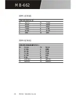
Serial Port COM1 (CN32), COM3 (CN30)
and COM4 (CN31) Connectors

The availability of this interface allows connection of serial devices
such as mouse, printer, etc.. Pin definitions as follows:

COM3 RS-232 (

CN30

)

Pin

Signal

Pin

Signal

1

NRLSD2

6

NCTS2

2

NDSR2

7

NDTR2

3

NRXD2

8

NRI2

4

NRTS2

9

GND

5

NTXD2

10

GND

Summary of Contents for MB-662

Page 1: ...hassis Caution Always ground yourself to remove any static charge before touching the CPU card Modern electronic devices are very sensitive to static electric charges As a safety precaution use a grou...

Page 2: ...6 Location of Jumpers Connectors JP13 CN16 CN9 CN12 CN8 JP18 CN7 JP16 JP7 JP3 JP17 DIMM1 DIMM2 JP14 JP15 CN21 CN13 CN6 CN11 CN35 CN37 CN36 CN33 CN32 CN30 CN22 CN3 CN10 CN14 JP10 JP1 CN2 CN25 CN17 CN24...

Page 3: ...pers Label Function JP1 Clear CMOS Selection JP2 Power ON Switch JP3 Panel Type Selection JP6 LCD Panel Voltage Setting JP7 LCD Clock Signal Selection JP8 Ethernet Tx Rx Link LED Connector JP10 COM4 R...

Page 4: ...N9 FPC Floppy Drive Connector CN10 Parallel Port 1 Connector CN11 Keyboard and Mouse Connector CN13 CPU Fan Power Connector CN14 RJ 45 Ethernet Connector CN16 Primary IDE Hard Drive Connector CN17 Sec...

Page 5: ...ways place jumper on protect mode In clearing CMOS place jumper for just a second follow clear CMOS illustration then immediately return jumper to protect mode Protect Clear CMOS 1 2 3 1 2 3 Default L...

Page 6: ...settings illustrated as follows Shift Clock AShift Clock 1 2 3 1 2 3 Default Ethernet Tx Rx Link LED Connector JP8 With ethernet Tx Rx Link LED indicator the ethernet status can be trace up through LE...

Page 7: ...settings are illustrated as follows RI Function 5Vout 12Vout 1 3 5 1 3 5 1 3 5 2 4 6 2 4 6 2 4 6 RS 232 RS 422 RS 485 7 9 11 7 9 11 7 9 11 8 10 12 8 10 12 8 10 12 Default Speaker Buzzer JP12 This onb...

Page 8: ...rly warning indicator and as well as a quick troubleshooting indicator Just follow the pin definition for each 7 LEDs illustrated below Pin Signal Pin Signal 1 Power_ON LED 2 Vcc 3 CPU_fan LED 4 Vcc 5...

Page 9: ...consumption and an increase in reliability The DiskOnChip is a small plug and play Flash disk It is easy to use And it saves integration overhead The DiskOnChip 2000 family of products is available i...

Page 10: ...s Just refer to the pin definitions below Pin Signal Pin Signal 1 Vcc 2 GND 3 N C 4 N C 5 N C 6 N C 100 66 Mhz Frequency Selection JP17 Provide the users to manually select the operating frequency wit...

Page 11: ...al 1 N C 11 N C 2 N C 12 12V 3 GND 13 GND 4 5V 14 PON 5 GND 15 GND 6 5V 16 GND 7 GND 17 GND 8 N C 18 5V 9 5VSB 19 5V 10 12V 20 5V Display Connectors CN3 and CN12 The MB 662 s PCI SVGA interface can dr...

Page 12: ...rd conventional D sub connector is equipped to interface with conventional CRT displays Refer to pin definitions as follows Pin Signal 1 RED 2 GREEN 3 BLUE 4 N C 5 Chassis GND 6 Chassis GND 7 Chassis...

Page 13: ...ion of the VGA interface is done completely via the software utility You do not have to set any jumpers Pin Signal Pin Signal 1 12 VDC 2 12 VDC 3 GND 4 GND 5 5 VDC 6 5 VDC 7 ENAVEE 8 GND 9 P0 10 P1 11...

Page 14: ...connector It acquires the new generation of plug and play Hot Plugging feature for both low speed and high speed devices It could also be expanded up to 127 connections through USB hub Refer pin defin...

Page 15: ...pin flat cable connector into CN7 Make sure that the red or blue wire corresponds to pin 1 on the connector No wor ries for CN9 FPC connector it s guided design for error free con nection 2 Attach the...

Page 16: ...24 WRITE GATE 25 GND 26 TRACK 0 27 GND 28 WRITE PROTECT 29 GND 30 READ DATA 31 GND 32 HEAD SELECT 33 GND 34 DISK CHANGE Note Please refer to the next page for CN9 pin definitions IrDA Connector CN8 H...

Page 17: ...Port 1 Connector CN10 and Parallel Port 2 Connector CN21 The mainboard is designed to support two parallel ports Port 1 connector CN10 also designated as LPT1 is a standard 25 pin D sub connector spe...

Page 18: ...11 BUST 12 PE 13 SLCT 14 AUTOFD 15 ERR 16 INIT 17 SLCTINI 18 GND 19 GND 20 GND 21 GND 22 GND 23 GND 24 GND 25 GND 26 GND Parallel Port 2 Connector CN21 13x2 pin header Pin Signal Pin Signal 1 STB 2 A...

Page 19: ...tor Pin Signal Pin Signal 1 KB DATA 7 MS DATA 2 MS DATA 8 N C 3 GND 9 GND 4 Vcc 10 Vcc 5 KB CLOCK 11 MS CLOCK 6 MS CLOCK 12 N C CPU and System Fan Power Connector CN13 and CN24 Two 3 pin plug in and e...

Page 20: ...tor CN14 MB 662 is outfitted with a standard RJ 45 LAN connector With support from Realtek RTL8139C chipset using either 10Mbs or 100Mbs are possible through it s N way auto negotiation featured opera...

Page 21: ...n the drive size 1 8 and 2 5 drives need one 44 pin to two 44 pin flat cable connector 3 5 drives use one 44 pin to two 40 pin connector Wire number 1 on the cable is normally red or blue and the othe...

Page 22: ...10 9 DATA 4 10 DATA 11 11 DATA 3 12 DATA 12 13 DATA 2 14 DATA 13 15 DATA 1 16 DATA 14 17 DATA 0 18 DATA 15 19 SIGNAL GND 20 N C 21 N C 22 GND 23 IO WRITE 24 GND 25 IO READ 26 GND 27 IO CHANNEL READY...

Page 23: ...6 DATA 9 7 DATA 5 8 DATA 10 9 DATA 4 10 DATA 11 11 DATA 3 12 DATA 12 13 DATA 2 14 DATA 13 15 DATA 1 16 DATA 14 17 DATA 0 18 DATA 15 19 SIGNAL GND 20 N C 21 N C 22 GND 23 IO WRITE 24 GND 25 IO READ 26...

Page 24: ...initions are list ed as follows SerialPortCOM2RS 232 CN22 Pin Signal Pin Signal 1 NRLSD1 6 NDSR1 2 NRXD1 7 NRTS1 3 NTXD1 8 NCTS1 4 NDTR1 9 NRI1 5 GND 10 GND LCD Inverter Backlight Power Connector CN25...

Page 25: ...GPO19 bit3 GPO20 bit4 The pin definitions are illustrated below Pin Signal Pin Signal 1 DIO_IN1 2 DIO_IN2 3 DIO_IN3 4 DIO_IN4 5 DIO_OUT1 6 DIO_OUT2 7 DIO_OUT3 8 DIO_OUT4 9 Vcc 10 GND Serial Port COM1...

Page 26: ...232 CN32 Pin Signal Pin Signal 1 DCDA 6 DSRA 2 RXDA 7 RTSA 3 TXDA 8 CTSA 4 DTRA 9 DTRA 5 GND 10 GND COM4 CN31 COM4RS 232 422 485 CN31 Pin Signal Pin Signal 1 DCDB 2 DSRB 3 RXDB 4 RTSB 5 TXDB 6 CTSB 7...

Page 27: ...ick MIDI Port Connector CN33 Pin Signal Pin Signal 1 Vcc 9 Vcc 2 JF0 10 JF2 3 JRC0 11 JRC2 4 GND 12 MOUT 5 GND 13 JRC3 6 JRC1 14 JF3 7 JF1 15 MIN 8 Vcc Audio Connector for CD_IN CN34 Links audio conne...

Page 28: ...standard form of connection for the users too Pin definitions as follows Line_OUT Phone Jack CN35 Pin Signal 1 GND 2 Line_OUT Left 3 GND 4 GND 5 Line_OUT Right Phone Jack for MIC CN36 A standard phon...

Page 29: ...for Line_IN CN37 The MB 662 is designed with line_OUT and for additional ease a line_IN connection is definitely needed It also comes with stan dard easy connection Pin definitions below Line_IN Phon...

Page 30: ...MB 662 3 0 MB 662 Installation GuideBC 599 596...

Reviews: