background image

Chapter 3  Award BIOS Setup    51

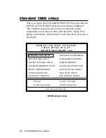
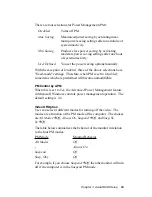
R O M   P C I / I S A   B I O S   ( 2 A 5 I I A K 9 )

S T A N D A R D   C M O S   S E T U P

A W A R D   S O F T W A R E ,   I N C .

Date (mm:dd:yy) : Fri, April 16, 1998
Time (hh:mm:ss) : 8:20:23

HARD DISKS

          CYLS       HEAD      PRECOMP     LANDZ     SECTOR     MODE

Drive  C:  Auto  (0b)

:     0

  0

     0              0         0           AUTO

Drive  D:  Auto  (0b)

:     0

       0        0

       0         0           AUTO

Drive A : 1.44M, 3.5 in.
Drive B : None
LCD & CRT : Both
Panel: 640x480  18BIT  TFT

Base Memory

: 640K

Extended Memory

: 27648K

Other Memory

: 384K

Total Memory

: 28672K

ESC: Quit

áâàß

 :Select Item

PU/PD/+/-:Modify

F1:Help

(Shift)F2:Change Color

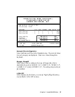
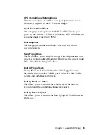
Date and Time Configuration

Select the Date and Time in the Standard setup.  The current values
for each category are displayed.  Enter new values through the
keyboard.

Floppy A, Floppy B

Select these icons to configure the type of floppy drive that is
attached to the system: 360 KB 5 1/4", 1.2 MB 5 1/4", 720 KB 3 1/2",
1.44 MB 3 1/2", and/or 2.88 MB 3 1/2".  The settings have not been
pre-installed.

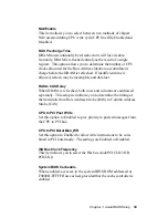
LCD & CRT

In the display selection item, you can use PageUp/PageDown key
to select Both , LCD, CRT or Auto.

Summary of Contents for PCM-5892

Page 1: ...PCM 5894 PCM 5892 All in One Single Board Pentium Computer with SVGA Ethernet and 4 serial ports...

Page 2: ...PART 15 OF THE FCC RULES THESE LIMITS ARE DESIGNED TO PROVIDE REASON ABLE PROTECTION AGAINTST HARMFUL INTERFER ENCEWHEN THE EQUIPMENT IS OPERATED IN A COMMERCIAL ENVIRONMENT THIS EQUIPMENT GENER ATES...

Page 3: ...c AMI is a trademark of American Megatrends Inc Award is a trademark of Award Software International Inc Cyrix is a trademark of Cyrix Corporation IBM PC AT PS 2 and VGA are trademarks of Internationa...

Page 4: ...hase an optioanl cable kit PCM 10489 3 P N 9979048900 If any of these items are missing or damaged contact your distribuitor or sales representative immediately Notice Dear Customer Thank you for purc...

Page 5: ...from P8 by counting the number of red wire Many times there are also markings on these two plugs indicating which is which NOTE Without any aditional devices PCM 5894 5892 alone is 5V operational 5V...

Page 6: ...ers 14 CPU installing and upgrading 15 Installing DRAM SIMMs 16 Installing SIMMs 16 Internal VGA setting J1 for PCM 5892 chipset only 17 System clock setting J2 18 LCD driving voltage select J3 and J1...

Page 7: ...Floppy drive connector CN16 37 Connecting the floppy drive 37 Floppy drive connector CN16 38 DiskOnChip socket U16 39 DiskOnChip DOC 2000 Installation 40 CPU jumper setting example 41 Chapter 3 AMIBIO...

Page 8: ...2 86 Windows NT 3 51 88 Windows NT 4 0 89 Chapter 5 SiS 5598 VGA Drivers For PCM 5892 only 91 System Requirements 92 Windows 95 92 WINDOWS 95 Display driver installation 92 Selecting resolution color...

Page 9: ...ion 99 Ethernet software configuration 100 Appendix A Programming the Watchdog Timer 101 Programming the watchdog timer 102 How to program the WATCHDOG TIMER 102 Demo program 103 Appendix B Installing...

Page 10: ......

Page 11: ...Chapter 1 General Information 1 1 General Information This chapter gives background informa tion on the mainboard Sections include Board specifications Layout and dimensions C H A P T E R...

Page 12: ...e keyboard PS 2 mouse interface The built in high speed PCI IDE controller supports both PIO and bus master modes Up to two IDE devices can be connected including large hard disks CD ROM drives tape b...

Page 13: ...00AFR Cyrix IBM 6x86MX PR166 266GPandIDTwinchipC6180 225MHz DiskOnChip SSD up to 72MB C T 65554 LCD controller supports 36 bit TFT panels 10Base T 100Base TX Ethernet supports remote boot ROM function...

Page 14: ...rts Multi word DMA and Ultra DMA 33 FDD interface Supports up to two floppy disk drives Multi mode parallel port Configured to LPT1 LPT2 LPT3 or disabled Supports SPP ECP and EPP Serial ports Three RS...

Page 15: ...ports up to 1024 x 768 64K colors Ethernet controller Realtek RTL8139 10Base T 100Base TX Ethernet controller SSD interface One 32 pin DIP socket for M Systems DiskOnChip 2000 series memory capacity f...

Page 16: ...6 PCM 5894 5892 User Manual Board layout U 1 U M C U M 8 6 6 3 B F 2 0 P M T 0 4 A SiS 5598 5582 BAT RTL8139 iTE I T 8 6 6 1 F D i s k O n C h i p CHIPS B5554...

Page 17: ...Chapter 1 General Information 7 Dimensions in mm PCM 5894 5892 dimensions 5 08 40 64 97 16 100 97 119 38 3 56 174 63 177 17 193 04 203 20 198 12 5 08 9 53 135 89 95 25 146 05 140 97 Board dimensions...

Page 18: ...8 PCM 5894 5892 User Manual...

Page 19: ...pter describes how to set up the main board hardware including instruc tions on setting jumpers and connecting peripherals switches and indicators Be sure to read all the safety precautions before you...

Page 20: ...jumpers and connectors Jumpers Label Function J1 Internal VGA setting J2 System clock setting J3 LCD driving voltage select J5 LCD SHF clock setting J6 LCD ASHF clock setting J7 Clear CMOS J8 CPU fre...

Page 21: ...r CN8 Auxilliary power connector 5V 12V CN9 Keyboard and mouse connector CN10 IrDA connector CN11 IDE hard drive connector CN12 Main power connector CN13 Printer port connector CN14 Ethernet 100 10Bas...

Page 22: ...12 PCM 5894 5892 User Manual U1 Locating jumpers J12 J19 J2 J8 J10 J13 J11 J7 J3 J16 J15 J14 J5 J6 J1 J21 J17 J20 J18...

Page 23: ...ion 13 U 1 UMC U M 8 6 6 3 B F 20PMT04A SiS 5 5 9 8 5 5 8 2 BAT RTL8139 iTE I T 8 6 6 1 F D i s k O n C h i p CHIPS B5554 Locating connectors CN10 CN11 CN13 CN12 CN9 CN16 CN15 CN14 CN2 CN5 CN8 CN6 U16...

Page 24: ...ins with the clip To open a jumper you remove the clip Sometimes a jumper will have three pins labeled 1 2 and 3 In this case you would connect either pins 1 and 2 or 2 and 3 The jumper settings are s...

Page 25: ...components can be dam aged by the sudden rush of power Only experi enced electronics personnel should open the PC chassis Caution Always ground yourself to remove any static charge before touching th...

Page 26: ...ired as one memory bank and both SIMMs must be the same size and type 1 Ensure that all power sources are disconnected 2 Slip the memory module into the socket at a 45 degree angle 3 Push the module t...

Page 27: ...5892 chipset only This jumpers is reserved for factory use The PCM 5894 PCM 5892 use different VGA chipset this jumper is used to select the relative onboard VGA chipset Internal VGA setting J1 PCM 5...

Page 28: ...clock and PCI clock You may need to adjust the CPU clock according to the base CPU speed CPU clock setting PCI J2 CPU 55MHz 27 5MHz 75MHz 32MHz 50MHz 33 3MHz 50MHz 25MHZ 60MHz 30MHz 66MHz 33MHz 40MHz...

Page 29: ...1 default LCD singal select J5 J6 You can select the LCD control signal by setting J5 J6 The following charts show the available option LCD Signal select J5 J6 SHF CLK ASHF CLK J5 J6 Clear CMOS J7 You...

Page 30: ...equency ratio J8 CPU frequency ratio J8 J8 P54C P55C AMD K6 1 5 3 5 3 5 2 0 2 0 2 0 2 5 2 5 2 5 3 0 3 0 3 0 default setting 4 0 4 5 5 5 5 0 1 3 5 2 4 6 1 3 5 2 4 6 1 3 5 2 4 6 1 3 5 2 4 6 1 3 5 2 4 6...

Page 31: ...elect J10 J10 must be set to match the CPU type between Dual Voltage e g P55C and Single Voltage e g P54C type CPU The chart below shows the proper jumper setting for their respective CPU type CPU typ...

Page 32: ...low shows the proper jumper settings for the respective Vcc CPU voltage setting 3 6v 3 5v 3 4v 3 3v 3 2v 3 1v 3 0v 2 9v 2 8v 2 7v 2 6v 2 5v 2 4v 2 3v 2 2V 2 1v default setting 8 2 7 1 8 2 7 1 8 2 7 1...

Page 33: ...er device s memory address J13 controls the memory address of the Flash disk DiskOnChip 2000 memory address J13 Memory address HEX J13 DISABLE DC00 D400 D000 CC00 D800 default setting These addresses...

Page 34: ...ts three sets of LED connectors for externalLEDs Ethernet active signal LED J14 J15 Flashing LEDs indicate that the PCM 5894 5892 is transmitting J14 or receiving J15 data Ethernet link signal LED J16...

Page 35: ...485 select COM2 Select J17 J18 RS 232 RS 422 RS 485 J17 J18 default COM3 COM4 IRQ select IRQ Selection J19 COM3 IRQ5 and COM4 IRQ10 COM3 IRQ10 and COM4 IRQ5 default 6 4 2 5 3 1 6 4 2 5 3 1 3 2 1 3 2 1...

Page 36: ...894 5892 User Manual COM3 COM4 RI pin voltage select J20 J21 COM3 RI pin setting J20 RI 5V 12V J20 COM4 RI pin setting J21 RI 5V 12V J21 6 4 2 5 3 1 6 4 2 5 3 1 6 4 2 5 3 1 6 4 2 5 3 1 6 4 2 5 3 1 6 4...

Page 37: ...is a 16 pin dual in line header used for conventional CRT displays A simple one to one adapter can be used to match CN1 to a standard 15 pin D SUB connector commonly used for VGA VGA display connector...

Page 38: ...7 ENAVEE 8 GND 9 P0 10 P1 11 P2 12 P3 13 P4 14 P5 15 P6 16 P7 17 P8 18 P9 19 P10 20 P11 21 P12 22 P13 23 P14 24 P15 25 P16 26 P17 27 P18 28 P19 29 P20 30 P21 31 P22 32 P23 33 P24 34 P25 35 SHF CLK 36...

Page 39: ...l Bus interfaces which give complete plug and play hot affach detach for up to 127 external devices The USB interfaces comply with USB specification Rev 1 0 and can be disabled in the system BIOS setu...

Page 40: ...ns for a speaker hard disk access indicator and an input switch for resetting the card Front panel connector CN6 Pin Signal 1 HDD LED Hard disk active 2 HDD LED VCC 3 Speaker 4 Speaker GND 5 GND 6 NC...

Page 41: ...Auxilliary power connector CN8 Pin Function 1 12V 2 GND 3 GND 4 5 V Main power connector CN12 Main power connector CN12 Pin Signal 1 GND 2 GND 3 N C 4 5 V 5 5 V 6 5 V Fan power connector CN2 and CN17...

Page 42: ...s especially in embedded applications a keyboard is not used The standard PC AT BIOS will report an error or fail during power on self test POST after a reset if the keyboard is not present The mainbo...

Page 43: ...s use a 1 x 44 pin to 2 x 40 pin connect Wire number 1 on the cable is red or blue and the other wires are gray 1 Connect one end of the cable to CN11 Make sure that the red or blue wire corresponds t...

Page 44: ...DATA 10 9 DATA 4 10 DATA 11 11 DATA 3 12 DATA 12 13 DATA 2 14 DATA 13 15 DATA 1 16 DATA 14 17 DATA 0 18 DATA 15 19 SIGNAL GND 20 N C 21 N C 22 GND 23 IO WRITE 24 GND 25 IO READ 26 GND 27 IO CHANNEL RE...

Page 45: ...le has a 26 pin connector on one end and a DB 25 connector on the other Parallel port IRQ The mainbaord supports one parallel port The port is designated as LPT1 and can be disabled or changed to LPT2...

Page 46: ...COM2 COM3 COM4 RS 232 422 485 serial port PIN SIGNAL PIN SIGNAL COM1 1 DCDA 2 DSRA 3 RXDA 4 RTSA 5 TXDA 6 CTSA 7 DTRA 8 RIA 9 GND 10 N C COM2 11 DCDB 12 DSRB 422TXD 485DATA 13 RXDB 14 RTSB 422TXD 485...

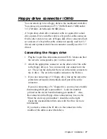
Page 47: ...to pin 1 on the connector 2 Attach the appropriate connector on the other end of the cable to the floppy drive s You can use only one connector in the set The set on the end after the twist in the ca...

Page 48: ...Y SELECT 3 GND 4 N C 5 GND 6 DRIVE TYPE 7 GND 8 INDEX 9 GND 10 MOTOR 0 11 GND 12 DRIVE SELECT 1 13 GND 14 DRIVE SELECT 2 15 GND 16 MOTOR 1 17 GND 18 DIRECTION 19 GND 20 STEP 21 GND 22 WRITE DATA 23 GN...

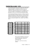
Page 49: ...om 2MB up to 72MB unformatted In order to manage the disk the DiskOnChip 2000 includes the TrueFFS M Systems Flash File System proprietary software The DiskOnChip 2000 package is pin to pin compatible...

Page 50: ...with thememorywindow Youshoulddisablethememoryshadowfrom the BIOS SETUP if the DOC cannot be accessed Configure DOC as a boot device To configure a DOC as a boot drive you should copy the operating s...

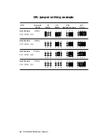
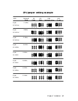
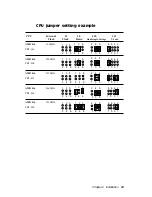
Page 51: ...Hz P54C 150 Intel Pentium 166MHz P54C 166 Intel Pentium 200MHz P54C 200 1 3 5 2 4 6 1 3 5 2 4 6 1 3 5 2 4 6 1 3 5 2 4 6 1 3 5 2 4 6 1 3 5 2 4 6 1 3 5 2 4 6 1 3 5 2 4 6 1 3 5 2 4 6 1 3 5 2 4 6 1 3 5 2...

Page 52: ...m 150MHz P55C PP MT 150 Intel Pentium 166MHz P55C PP MT 166 Intel Pentium 200MHz P55C PP MT 200 Intel Pentium 233MHz P55C PP MT 233 1 3 5 2 4 6 2 4 6 1 3 5 2 4 6 1 3 5 2 4 6 1 3 5 2 4 6 1 3 5 8 6 4 2...

Page 53: ...yrix 225MHz M2 PR266 Cyrix 233MHz M2 PR266 1 3 5 2 4 6 1 3 5 2 4 6 1 3 5 2 4 6 1 3 5 2 4 6 1 3 5 2 4 6 2 4 6 1 3 5 1 3 5 2 4 6 2 4 6 1 3 5 2 4 6 1 3 5 2 4 6 1 3 5 2 4 6 1 3 5 2 4 6 1 3 5 2 4 6 1 3 5 2...

Page 54: ...R75 AMD K5 90MHz PR90 AMD K5 100MHz PR100 AMD K5 90MHz PR120 AMD K5 100MHz PR133 1 3 5 2 4 6 1 3 5 2 4 6 1 3 5 2 4 6 2 4 6 1 3 5 2 4 6 1 3 5 2 4 6 1 3 5 2 4 6 1 3 5 2 4 6 1 3 5 1 3 5 2 4 6 1 3 5 2 4 6...

Page 55: ...MD K6 200MHz PR2 200 AMD K6 233MHz PR2 233 AMD K6 266MHz PR2 266 AMD K6 233MHz PR2 300 2 4 6 1 3 5 2 4 6 1 3 5 2 4 6 1 3 5 2 4 6 1 3 5 2 4 6 1 3 5 1 3 5 2 4 6 1 3 5 2 4 6 8 6 4 2 7 5 3 1 8 6 4 2 7 5 3...

Page 56: ...46 PCM 5894 5892 User Manual...

Page 57: ...Chapter 3 Award BIOS Setup 47 3 Award BIOS Setup This chapter describes how to configure the BIOS for the PCM 5894 5892 C H A P T E R...

Page 58: ...he message and press the F1 key to continue the bootup sequence System configuration verification These routines check the current system configuration against the values stored in the card s CMOS mem...

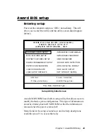
Page 59: ...at the information is retained when the power is turned off Many fields in the setup screens have on line help descriptions available press F1 to access this help Entering setup Power on the computer...

Page 60: ...can be accessed by pressing F1 CMOS setup screen R O M P C I I S A B I O S 2 A 5 I I A K 9 C M O S S E T U P U T I L I T Y A W A R D S O F T W A R E I N C ESC Quit Select Item F10 Save Exit Setup Shif...

Page 61: ...ory 27648K Other Memory 384K Total Memory 28672K ESC Quit Select Item PU PD Modify F1 Help Shift F2 Change Color Date and Time Configuration Select the Date and Time in the Standard setup The current...

Page 62: ...4 S 2 1 M L N T S D 0 0 6 x 0 0 8 s e Y s e Y C E N 0 1 3 3 C A 8 4 4 6 L N T F T 0 8 4 x 0 4 6 s t i b 2 1 s e Y s e Y a b i h s o T A 9 0 2 C 0 1 M T L 0 8 4 x 0 4 6 T F T s t i b 8 1 s e Y s e Y C...

Page 63: ...O S 2 A 5 I I A K 9 C M O S S E T U P U T I L I T Y A W A R D S O F T W A R E I N C ESC Quit Select Item F10 Save Exit Setup Shift F2 Change Color Virus Protection Boot Sequence STANDARD CMOS SETUP IN...

Page 64: ...Help PU PD Modify F5 Old Values Shift F2 Color F6 Load BIOS Defaults F7 Load Setup Defaults R O M P C I I S A B I O S 2 A 5 I I A K 9 B I O S F E A T U R E S S E T U P A W A R D S O F T W A R E I N C...

Page 65: ...for the operating system Swap Floppy Drive This item allows you to swap the floppy drive assignments so that drive A is treated as drive B and drive B is treated as drive A under DOS The default setti...

Page 66: ...s a password at boot up and Setup which only requires a password to access the setup utility Video BIOS Shadow Determines whether the video display card BIOS will be copied into system DRAM in order t...

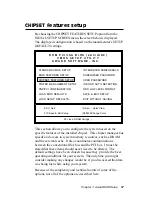
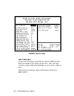
Page 67: ...ur system Because of the complexity and technical nature of some of the options not all of the options are described here CHIPSET features setup R O M P C I I S A B I O S 2 A 5 I I A K 9 C M O S S E T...

Page 68: ...CK Disabled NA Enable Disabled Starting Point of Paging 1T Refresh Cycle Time us 187 2 RAS Pulse Width Refresh 6T RAS Precharge Time 4T RAS to CAS Delay 4T CAS Pulse Width FP 2T CAS Pulse Width EDO 1T...

Page 69: ...and data lost RAS to CAS Delay When DRAM is refreshed both rows and columns are addressed separately This setup item allows you to determine the timing of the transition from Row Address Strobe RAS t...

Page 70: ...addressed at C0000H to C7FFFH to be cached if the cache controller is also enabled Memory Hole at 15M 16M In order to improve performance certain space in memory can be reserved for ISA cards The mem...

Page 71: ...ASSSWORD POWER MANAGEMENT SETUP IDE HDD AUTO DETECTION PNP PCI CONFIGURATION HDD LOW LEVEL FORMAT LOAD BIOS DEFAULTS SAVE EXIT SETUP LOAD SETUP DEFAULTS EXIT WITHOUT SAVING ESC Quit Select Item F10 Sa...

Page 72: ...d DPMS Supported Doze Speed div by 2 Stdby Speed div by 3 MODEM Use IRQ 3 Hot Key SMI Disabled PM Timers HDD Off After Disable Doze Mode Disable Standby Mode Disable Suspend Mode Disable PM Events COM...

Page 73: ...Disabled some items which are predefined will become unmodifiable PM Control by APM When this is set to Yes the Advanced Power Management feature in Microsoft Windows controls power management operati...

Page 74: ...Blank option DPMS Display Power Management System allows the BIOS to control the video display card if the card has the DPMS feature V H SYNC Blank Default BLANK non green monitor less saving DPMS Dis...

Page 75: ...e This sets the period of system inactivity after which the system goes into Standby mode the intermediate power saving state The settings range from 20 seconds to 40 minutes and can be set manually w...

Page 76: ...O device wants to gain the attention of the operating system it signals this by causing an IRQ Interrupt ReQuest to occur When the operating system is ready to respond to the request it interrupts its...

Page 77: ...I S A B I O S 2 A 5 I I A K 9 C M O S S E T U P U T I L I T Y A W A R D S O F T W A R E I N C STANDARD CMOS SETUP INTEGRATED PERIPHERALS BIOS FEATURES SETUP SUPERVISER PASSWORD CHIPSET FEATURES SETUP...

Page 78: ...uration Data Disabled IRQ 3 assigned to Legacy ISA IRQ 4 assigned to Legacy ISA IRQ 5 assigned to PCI ISA PnP IRQ 7 assigned to Legacy ISA IRQ 9 assigned to PCI ISA PnP IRQ 10 assigned to Legacy ISA I...

Page 79: ...ou should retain the default configuration unless advised by your system manufacturer The choices are Level Edge PCI IDE IRQ Map To This allows you to configure your system to the type of IDE disk con...

Page 80: ...refore unusable BIOS defaults will load automatically when you turn the PCM 5894 5892 on R O M P C I I S A B I O S 2 A 5 I I A K 9 C M O S S E T U P U T I L I T Y A W A R D S O F T W A R E I N C STAND...

Page 81: ...CTION PNP PCI CONFIGURATION HDD LOW LEVEL FORMAT LOAD BIOS DEFAULTS SAVE EXIT SETUP LOAD SETUP DEFAULTS EXIT WITHOUT SAVING ESC Quit Select Item F10 Save Exit Setup Shift F2 Change Color Onboard I O I...

Page 82: ...R D S O F T W A R E I N C IDE Primary Master Slave PIO This sets the hard disk PIO transfer mode which affects the hard disk data transfer rate The system will auto detect the PIO mode of a device in...

Page 83: ...lers Onboard Serial Port 1 2 3 4 You can set the I O address for serial ports 1 2 The system will auto detect the COM port address when this item set to Auto 3F8 IRQ4 default for port 1 2F8 IRQ3 defau...

Page 84: ...The setting options are SPP ECP EPP EPP ECP If you set this option to SPP or EPP the ECP Mode Use DMA option will not appear on the screen If you set this option to SPP or ECP the Parallel Port EPP Ty...

Page 85: ...ssword setting You can set either supervisor or user password or both of them The difference between the two is that the supervisor password allows unrestricted access to enter and change the options...

Page 86: ...isabled the system will boot and you can enter the utility freely STANDARD CMOS SETUP INTEGRATED PERIPHERALS BIOS FEATURES SETUP SUPERVISER PASSWORD CHIPSET FEATURES SETUP USER PASSSWORD POWER MANAGEM...

Page 87: ...RD CHIPSET FEATURES SETUP USER PASSSWORD POWER MANAGEMENT SETUP IDE HDD AUTO DETECTION PNP PCI CONFIGURATION HDD LOW LEVEL FORMAT LOAD BIOS DEFAULTS SAVE EXIT SETUP LOAD SETUP DEFAULTS EXIT WITHOUT SA...

Page 88: ...ility HARD DISK INSTALL FAILURE PRESS ANY KEY TO CONTINUE SIZE CYLS HEADS PRECOMP LANDZONE SECTOR MODE Drive C ob 0 0 0 0 0 0 AUTO Drive D ob 0 0 0 0 0 0 AUTO R O M P C I I S A B I O S 2 A 5 I I A K 9...

Page 89: ...This record is required for the system to operate R O M P C I I S A B I O S 2 A 5 I I A K 9 C M O S S E T U P U T I L I T Y STANDARD CMOS SETUP INTEGRATED PERIPHERALS BIOS FEATURES SETUP SUPERVISER P...

Page 90: ...TURES SETUP USER PASSSWORD POWER MANAGEMENT SETUP IDE HDD AUTO DETECTION PNP PCI CONFIGURATION HDD LOW LEVEL FORMAT LOAD BIOS DEFAULTS SAVE EXIT SETUP LOAD SETUP DEFAULTS EXIT WITHOUT SAVING ESC Quit...

Page 91: ...hapter 4 Driver Installation 81 4 C T 6555x Flat Panel CRT Controller Display Drivers and Utilities For PCM 5894 only This chapter provides information about Driver types and installation C H A P T E...

Page 92: ...s not require any special drivers to operate in standard modes The purpose of the enclosed software drivers is to take advantage of the extended features of the CHIPS VGA Flat Panel CRT controller Har...

Page 93: ...isk Understand the MS DOS directory structure If you are uncertain about any of these concepts please refer to the DOS or OS 2 user reference guides for more information before you proceed with the in...

Page 94: ...ies Inc Video Controller driver will appear highlighted in the Models list box Select Chips and Tech 65554 PCI new and click OK Click OK to start the driver installation 3 Once the installation is com...

Page 95: ...hen from the pull down menu choose Run At the Command Line prompt type cd rom CD ROM model name driver vga driver win31 setup exe Press the ENTER key or click OK to begin the installation cd rom the d...

Page 96: ...to the OS 2 drive Type A ENTER to make this default drive Type SETUP A C ENTER Where A is the floppy disk drive and C is hard disk partition containing OS 2 When the Setup Program is completed you wil...

Page 97: ...s select Primary Display and then select OK 5 When the Primary Display Driver List window appears select Chips and Technologies 65554 from the list of adapter types then select OK or install the video...

Page 98: ...click the Display Type buttom into the Display Type windows then click on Change buttom from the Adapter Type icon And click on Have Disk buttom in the change display window 2 Place the Supporting CD...

Page 99: ...r CD ROM dirve In the Select Device window click on Have Disk select Browse and find the NT 4 0 driver from cd rom CD ROM model name dirver vga driver win98 nt windows nt nt40 Oemsetup inf cd rom the...

Page 100: ...9 0 PCM 5894 5892 User Manual...

Page 101: ...Chapter 4 Driver Installation 91 5 SiS 5598 VGA Drivers C H A P T E R The content of this chapter includes SiS 5598 VGA Driver installation instructions for the PCM 5892 For PCM 5892 only...

Page 102: ...log box appears type the directory storing the drivers and click OK or click the Browse button to manually locate the drivers The directory is cd rom CD ROM PCM 5892 Driver vga driver win95 and the fi...

Page 103: ...on 640 x 480 256 colors Selecting resolution color depth and re fresh 1 Click on the Start button and select Control Panel from the Settings menu 2 Double click on the Display icon 3 Select the Settin...

Page 104: ...d there are 5 items in the program group Multimedia Manager SiS MMPlayer SVGA Setup Center Screen Uninstall 5 A setup successful dialog will apear when setup is completed and the user can choose to re...

Page 105: ...click on the Display icon 3 Select Change Display Type from Display Settings 4 Select Change from Display Type 5 Select Other from Select Device 6 Insert the Supporting CD ROM into your CD ROM drive...

Page 106: ...1280 x 1024 6 Select Test to test the resolution If the display test screen was good then select Yes when the Testing Mode dialog box appears If the display test screen was bad then select No Windows...

Page 107: ...ution and color depth 1 Click on the Start button and select Control Panel from the Settings group 2 Double click on the Display icon 3 Select Settings tab in the Display Properties window 4 In the Co...

Page 108: ...he AUTOEXEC BAT file or not Video Mode Setting A list of the different video modes that can be supported is displayed Be sure to first test the video mode by highlighting the mode and then by pressing...

Page 109: ...are Configuration 99 6 Ethernet Software configuration This chapter details the Ethernet software configuration information It shows you how to configure the card to match your application requirement...

Page 110: ...erface Just highlight the option you wish to change by using the Up and Down keys To change a selected item press Enter and a screen will appear with the available options Highlight your option and pr...

Page 111: ...hdog Timer The mainboard is equipped with a watchdog timer that resets the CPU or generates an interrupt if processing comes to a standstill for whatever reason This feature ensures system reliability...

Page 112: ...0x85 set interval to 5 minutes 2 To set the time out event output data to prot 0x444 0 reset system 1 2 3 IRQ 10 15 11 respectively 4 NMI e g outportb 0x444 0 set time out event to reset system 3 To...

Page 113: ...0x443 enable watchdog timer customer_job execute your job here be sure your job will finished within 10 seconds outportb 0x80 0 refresh watchdog timer otherwise the system will reset after time out o...

Page 114: ...104 PCM 5894 5892 User Manual...

Page 115: ...Appendix B Installing PC 104 Modules 105 B Installing PC 104 Modules This appendix provides instructions for installing PC 104 modules A P P E N D I X...

Page 116: ...PCM 3115B PCMCIA Module two slot PCM 3200 PC 104 Sound Module PCM 3420 PC 104 Fast SCSI Module PCM 3521 Advanced Flat Panel CRT VGA Module PCM 3522 LCD Panel Adapter PCM 3600 PC 104 Fax Modem Module P...

Page 117: ...already mentioned above Step2 Make any jumper or link changes required to the CPU card now Once the PC 104 module is mounted you may have difficulty in accessing these Step3 Mount the PC 104 module on...

Page 118: ...108 PCM 5894 5892 User Manual 0 200 0 0 0 200 3 350 3 550 0 200 3 575 3 250 0 300 3 775 3 575 PC 104 module dimenstions inches 5...

Page 119: ...Appendix C Optional Extras 109 C Optional Extras A P P E N D I X...

Page 120: ...t a n i m r e T 0 5 3 0 4 4 1 0 7 1 E D I 8 1 d n a 5 2 m m 0 5 3 C D I e l a m e f m m 2 n i p 4 4 0 0 5 0 4 4 1 0 7 1 P 0 4 E D I 5 3 m m 0 0 5 C D I e l a m e f m m 4 5 2 n i p 0 4 0 0 7 0 4 3 1 0...

Reviews: