ccTalk Paylink Lite 2 User Manual
Aardvark Embedded Solutions Ltd.
Issue 1.1
3
rd
August 2018
Page 7
3.2 J0102
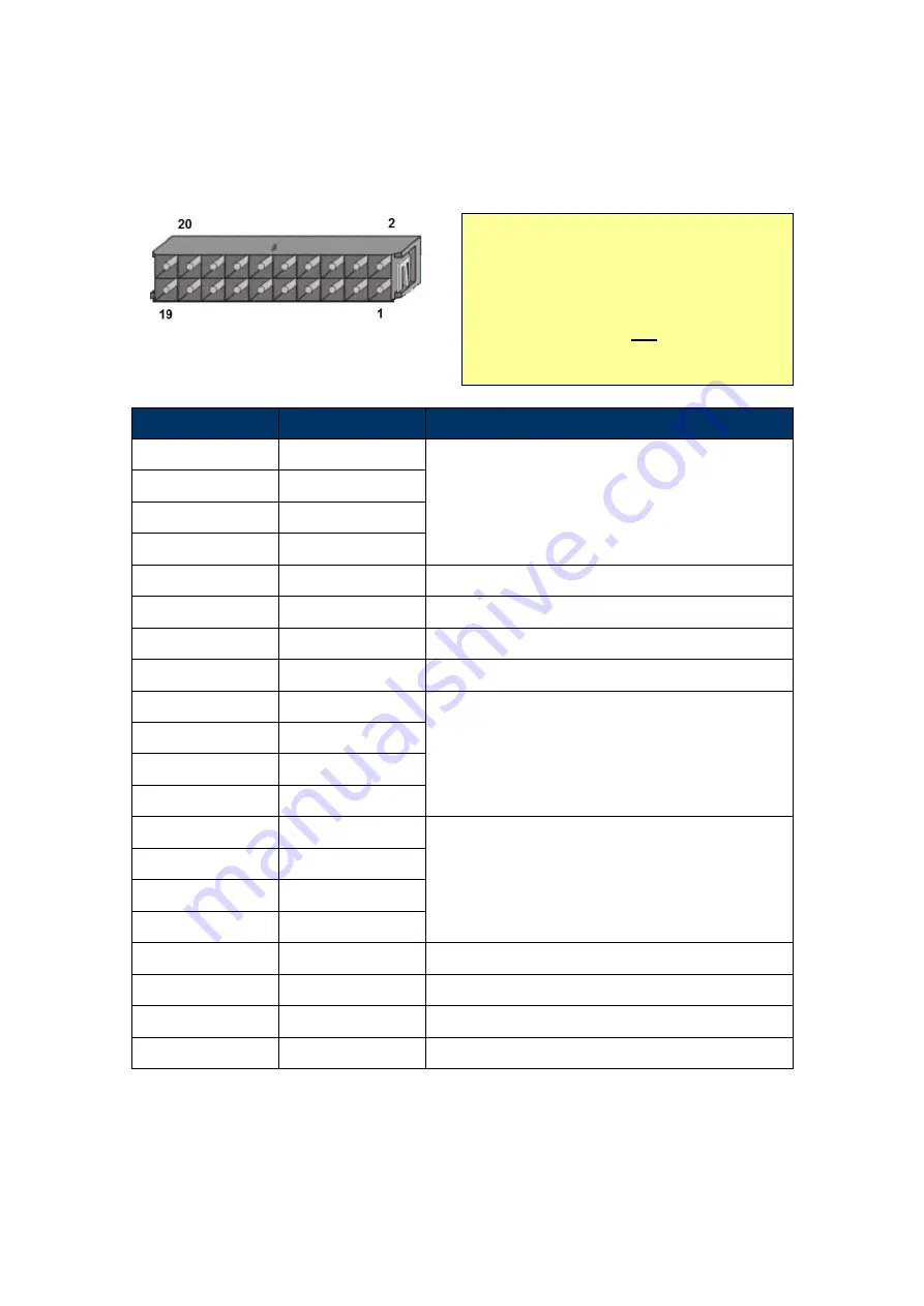
– Digital I/O Connector
The pinout of the I/O connector on all Paylink Lite 2 boards is the same.
Board Edge
In order to maintain compatibility with
earlier versions of Paylink, the pin
allocation of this connector is as
shown in the diagram to the left.
Note that this does not match the pin
allocation described in the Molex
Microfit documentation.
Pin
Signal Name
Description
1
+12 VF
Twelve Volt (Fused) signals for use with
output signals.
2
+12 VF
3
+12 VF
4
+12 VF
5
Output 0
Output signal 0 (Active Low).
6
Output 1
Output signal 1 (Active Low).
7
Output 2
Output signal 2 (Active Low).
8
Output 3
Output signal 3 (Active Low).
9
Pull-Up 0
Pull-ups to the USB 5V to allow the direct
driving of LEDs.
10
Pull-Up 1
11
Pull-Up 2
12
Pull-Up 3
13
Ground
Ground reference signals for use with
input signals.
14
Ground
15
Ground
16
Ground
17
Input 0
Switch input 0.
18
Input 1
Switch input 1.
19
Input 2
Switch input 2.
20
Input 3
Switch input 3.


