background image

Publication No. 500-657806-000 Rev. G

Connectors and Pinouts 59

A.7  PMC Connector Pinout

A.7.1 PMC #1 (J11)/PMC #2 (J21) Connector and Pinout

The PCI Mezzanine Card (PMC) carries the same signals as the PCI standard; 
however, the PMC standard uses a completely different form factor. 

Table A-2


through 

A-5

 are the pinouts for the PMC connectors.

Signal names are generic labels. J11 signals are for the PCI1 bus and J21 signals are 
for the PCI0 bus.

Table A-2 PMC #1 (J11)/PMC #2 (J21) Connector Pinout

PMC Connector (J11/J21)

PMC Connector (J11/J21)

Left Side

Right Side

Left Side

Right Side

Pin

Name

Pin

Name

Pin

Name

Pin

Name

1

GND

2

-12V

33

FRAME#

34

GND

3

GND

4

INTA#

35

GND

36

IRDY#

5

INTB#

6

INTC#

37

DEVSEL#

38

+5 V

7

BMODE1A

8

+5 V

39

PCIXCAP

40

LOCK#

9

INTD#

10

NC

41

SDONE#

42

NC

11

GND

12

NC

43

PAR

44

GND

13

CLK

14

GND

45

VCC_3.3

46

AD[15]

15

GND

16

GNT[1]#

47

AD[12]

48

AD[11]

17

REQ#

18

+5 V

49

AD[9]

50

+5 V

19

VCC_3.3

20

AD[31]

51

GND

52

C/BE#[0]

21

AD[28]

22

AD[27]

53

AD[6]

54

AD[5]

23

AD[25]

24

GND

55

AD[4]

56

GND

25

GND

26

C/BE#[3]

57

VCC_3.3

58

AD[3]

27

AD[22]

28

AD[21]

59

AD[2]

60

AD[1]

29

AD[19]

30

+5 V

61

AD[0]

62

+5 V

31

VCC_3.3

32

AD[17]

63

GND

64

REQ64#

Summary of Contents for CPCI-7806

Page 1: ...I 7806RC Pentium Celeron M Universal CompactPCI Single Board Computer THE CPCI 7806RC IS DESIGNED TO MEET THE EUROPEAN UNION EU RESTRICTIONS OF HAZARDOUS SUBSTANCE RoHS DIRECTIVE 2015 863 CURRENT REVISION Publication No 500 657806 000 Rev G ...

Page 2: ...0006421 D E January 2018 Change Number ECO 00009844 F July 2011 Change Number ECO 00013936 G March 2018 Rebranded to Abaco Systems Abaco Systems is registered with an approved Producer Compliance Scheme PCS and subject to suitable contractual arrangements being in place will ensure WEEE is processed in accordance with the requirements of the WEEE Directive Abaco Systems will evaluate requests to t...

Page 3: ... D subscript and binary numbers have a b subscript The prefix 0x shows a hexadecimal number following the C programming language convention Thus One dozen 12D 0x0C 1100b The multipliers k M and G have their conventional scientific and engineering meanings of x103 x106 and x109 respectively and can be used to define a transfer rate The only exception to this is in the description of the size of mem...

Page 4: ... related to CPCI 7806 CPCI 7806RC VxWorks Board Support Package Abstraction BSPX ACC 0584 ACC 0584RC Installation Guide CPCI 7806RC Datasheet ACC 0584RC Datasheet Third party Documents PCI Local Bus Specification Rev 2 2 CMC Specification P1386 Draft 2 0 PMC Specification P1386 1 Draft 2 0 CompactPCI Specification PICMG 2 0 R3 0 Packet Switching Backplane Specification PICMG 2 16 R1 0 The I2C Spec...

Page 5: ...C has been evaluated to and has met the requirements for compliance to the following standards International Compliance EN55022 1998 CISPR 22 1997 IEC61000 4 2 IEC61000 4 3 IEC61000 4 4 IEC61000 4 5 IEC61000 4 6 European Union CE Mark BS EN55024 1998 w A1 01 A2 03 BS EN55022 Class A United States FCC Part 15 Subpart B Section 109 Class A Australia New Zealand AS NZS CISPR 22 2002 Class A Canada IC...

Page 6: ...rence when the equipment is operated in a commercial environment This equipment generates uses and can radiate radio frequency energy and if not installed and used in accordance with the instruction manual may cause harmful interference to radio communications Operation of this equipment in a residential area is likely to cause harmful interference in which case the user will be required to correc...

Page 7: ...in the Technical Support database and allocate it a unique Case number for use in any future correspondence Alternatively you may also contact Abaco s Technical Support via LINK support abaco com Returns If you need to return a product there is a Return Materials Authorization RMA form available via the website Support page LINK https www abaco com support Do not return products without first cont...

Page 8: ...aphics Adapter 37 3 Embedded PC RTOS Features 38 3 1 CompactPCI Bus Bridge 38 3 1 1 PCI Interface 38 3 1 2 Buffer Architecture 38 3 1 3 Configuration Register and Control Status Registers CSRs 38 3 1 4 Transaction Forwarding 39 3 2 Watchdog Timer 39 3 2 1 General 39 3 2 2 Function 39 3 2 3 Registers 41 3 2 4 Register Unlocking Sequence 48 3 2 5 Reload Sequence 48 3 3 CompactFlash 48 3 3 1 Configur...

Page 9: ...onal Software Driver Installation 79 D 2 1 Video Driver Installation 79 D 2 2 Hance Rapids Chipset Software Installation 79 D 2 3 USB 2 0 EHCI Host Controller 79 D 2 4 Ethernet Adapter Drivers Installation 80 E 1 Standard IPMI Commands 81 E 1 1 Get Device ID 81 E 2 Cold Reset 82 E 3 Warm Reset 82 E 3 1 Get Self Test Results 82 E 3 2 SetACPI Power State 83 E 3 3 Get ACPI Power State 83 E 3 4 Get De...

Page 10: ...a PMC Card on the CPCI 7806 CPCI 7806RC 23 Figure 1 3 Front Panel LED Positions 25 Figure 2 1 Connections for the PC Interrupt Logic Controller 34 Figure 3 1 Watchdog Timer Block Diagram 40 Figure 3 2 Typical System Configuration 49 Figure A 1 J1 Connector and Pinout 53 Figure A 2 J2 Connector and Pinout 54 Figure A 3 J3 Connector and Pinout 55 Figure A 4 J5 Connector and Pinout 56 Figure A 5 Ethe...

Page 11: ...ster DS 42 Table 3 9 Revision Identification Register RID 43 Table 3 10 Programming Interface Register PI 43 Table 3 11 Sub Class Code Register SCC 43 Table 3 12 Base Code Class Register BCC 43 Table 3 13 Header Type Register HEDT 43 Table 3 14 Base Address Register 1 BAR1 43 Table 3 15 Details of Base Address Register 1 BAR1 43 Table 3 16 Subsystem Vendor ID SVID 44 Table 3 17 Subsystem ID SID 44...

Page 12: ...6 Table E 1 NetFn 0x06 Cmd 0x01 81 Table E 2 NetFn 0x06 Cmd 0x02 82 Table E 3 NetFn 0x06 Cmd 0x03 82 Table E 4 NetFn 0x06 Cmd 0x04 82 Table E 5 NetFn 0x06 Cmd 0x06 83 Table E 6 NetFn 0x06 Cmd 0x07 83 Table E 7 NetFn 0x06 Cmd 0x08 84 Table E 8 NetFn 0x06 Cmd 0x52 84 Table E 9 NetFn 0x04 Cmd 0x00 85 Table E 10 NetFn 0x04 Cmd 0x01 85 Table E 11 NetFn 0x04 Cmd 0x2D 86 Table E 12 NetFn 0x0A Cmd 0x10 87...

Page 13: ...y drive support requires ACC 0584 ACC 0584RC USB 2 0 requires ACC 0584 ACC 0584RC Two RS232 serial ports COM1 via front panel COM2 via ACC 0584 ACC 0584RC Real Time clock calendar Front panel reset switch Miniature speaker Keyboard Mouse port requires ACC 0584 ACC 0584RC The 855GME chipset allows the CPCI 7806 CPCI 7806RC to provide enhanced features such as integrated video and Ultra ATA 100 IDE ...

Page 14: ...ctPCI bus The CPCI 7806 CPCI 7806RC are capable of executing many of today s embedded operating systems such as VxWorks or QNX The embedded features of the CPCI 7806 CPCI 7806RC are described in Chapter 3 Embedded PC RTOS Features page 38 of this manual The CPCI 7806 CPCI 7806RC are suitable for use in applications ranging from telecommunications simulation instrumentation industrial control proce...

Page 15: ...l CompactPCI Connector CompactPCI Connector CompactPCI Connector IPMI 64 66 PCI Bus Universal PCI to PCI Bridge PCI Mezzanine Expansion Site CompactPCI Connector CompactPCI Bus PMC I O Intel 82546EB Dual Ethernet Controller PICMG 2 16 Interface SWX Front Panel Ethernet Ethernet Front Panel Notes Intel 82546GB Dual Ethernet Controller is for CPCI 7806 RoHS product only Pentium M Processor or Celero...

Page 16: ...ion of any electrical system in such an environment constitutes a definite safety hazard Keep Away from Live Circuits Operating personnel must not remove product covers Component replacement and internal adjustments must be made by qualified maintenance personnel Do not replace components with power cable connected Under certain conditions dangerous voltages may exist even with the power cable rem...

Page 17: ...damage that might have occurred during shipment The board s should be checked for broken components damaged printed circuit board s heat damage and other visible contamination All claims arising from shipping damage should be filed with the carrier and a complete report sent to Abaco Customer Care 1 3 Handling Precaution Electronic assemblies use devices that are sensitive to static discharge Obse...

Page 18: ...r jumpers The physical location of the jumpers and connectors for the single board computers SBCs are illustrated in Figure 1 1 on page 19 The definitions of the SBC board jumpers and connectors are included in Table 1 1 through Table 1 3 Please note that the CPCI 7806 CPCI 7806RC offer two PMC sites designated PMC 1 and PMC 2 as shown in Figure 1 1 on page 19 CAUTION All jumpers marked User Confi...

Page 19: ...Publication No 500 657806 000 Rev G Handling and Installation 19 Figure 1 1 CPCI 7806 CPCI 7806RC PMC and Jumper Locations PMC 1 PMC 2 ...

Page 20: ... hold jumper in place for shipping Table 1 1 SBC Board Connectors Connector Function J1 J2 CompactPCI J3 COM2 Floppy J5 USB IDE SATA PMC I O J6 J7 Ethernet 1 Ethernet 2 J8 COM 1 J11 J12 J13 J14 PMC Slot 1 J21 J22 PMC Slot 2 J25 ITP E2 Hotswap Switch E3 Battery E4 CMOS Clear and Boot Continuation Table 1 2 Battery Enable User Configurable Jumper E3 Select Jumper Position 1 3 Jumper Position 2 4 Bat...

Page 21: ...assword 1 Turn off power to the unit 2 Place a jumper on E4 pins 1 and 2 3 Wait approximately 5 seconds 4 Remove jumper from E4 pins 1 and 2 5 Power up the unit When power is reapplied to the unit the CMOS password will have been cleared and the CMOS will be set to its defaults values ...

Page 22: ...nit is to be greater than 400 LFM 3 Insert the CPCI 7806 CPCI 7806RC into a CompactPCI chassis system controller or peripheral slot While ensuring that the board is properly aligned and oriented in the supporting board guides slide the board smoothly forward against the mating connector Use the ejector handles to firmly seat the board 4 All needed peripherals can be accessed from the front panel o...

Page 23: ...ecial non volatile battery backed memory chip and are collectively referred to as the board s CMOS Configuration The CMOS configuration controls many details concerning the behavior of the hardware from the moment power is applied Details of the CPCI 7806 CPCI 7806RC BIOS setup program are included in BIOS Setup Utility on page 63 Figure 1 2 Installing a PMC Card on the CPCI 7806 CPCI 7806RC PMC E...

Page 24: ...GA Serial ATA port LVDS COM1 COM2 Keyboard Mouse PMC I O for one expansion site IDE drive floppy drive and two USB ports These signals are accessed by the use of a rear panel transition board such as the ACC 0584 ACC 0584RC which terminates into industry standard connectors The front panel connectors including connector pinouts and orientation for the CPCI 7806 CPCI 7806RC are defined in Connector...

Page 25: ...ED Definition Figure 1 3 Front Panel LED Positions RST CompactPCI L A N 1 TM S M E Z Z A N I N E C A R D M E Z Z A N I N E C A R D C O M 1 L A N 2 Switch LED 1 LED 3 LED 2 LAN Active 10BASE T LED 4 PMC 1 PMC 2 LAN Active 100BASE TX 1000BASE T 10BASE T 100BASE TX 1000BASE T ...

Page 26: ...s serial ports USB ports IDE drives floppy drives video controller and Ethernet controller are all memory mapped the same as similarly equipped desktop systems ensuring compatibility with modern operating systems The following sections describe the standard features of the CPCI 7806 CPCI 7806RC 2 1 CPU The CPCI 7806 CPCI 7806RC CPU is factory populated with a Pentium M or Celeron M processor The C...

Page 27: ... Memory can be accessed as bytes words or longwords The CPCI 7806 CPCI 7806RC accepts one 200 pin DDR SDRAM SODIMM along with onboard memory for a maximum capacity of 1 Gbytes The onboard DRAM is accessible to the CompactPCI bus through the PCI to PCI bridge and is addressable by the local processor NOTE Memory capacity may be extended as parts become available ...

Page 28: ...ce The BIOS initializes and configures all these registers properly adjusting these I O ports directly is not normally necessary The assigned and user available I O addresses are summarized in the I O Address Map Table 2 1 Table 2 1 CPCI 7806 CPCI 7806RC I O Address Map I O ADDRESS RANGE SIZE IN BYTES HW DEVICE PC AT FUNCTION 000 00F 16 DMA Controller 1 Intel 8237A Compatible 010 01F 16 Reserved 0...

Page 29: ... I O Used for IPMI 3F0 3F7 8 Super I O Chip Primary Floppy Disk Controller 3F8 3FE 7 Super I O Chip COM1 Serial I O 16550 Compatible 3FF 4FF 256 Reserved 500 CFF 2048 Reserved While these I O ports are reserved for the listed functions they are not implemented on the CPCI 7806 CPCI 7806RC They are listed here to make the user aware of the standard PC usage of these ports Table 2 1 CPCI 7806 CPCI 7...

Page 30: ...e IBM PC AT computer added eight more IRQx lines numbered IRQ8 to IRQ15 by cascading a second slave PIC into the original master PIC IRQ2 at the master PIC was committed as the cascade input from the slave PIC This architecture is represented in Figure 2 1 on page 34 To maintain backward compatibility with PC XT systems IBM chose to use the new IRQ9 input on the slave PIC to operate as the old IRQ...

Page 31: ...cessor Error 11 17 System Configuration Check Same as Real Mode 12 18 Memory Size Check Same as Real Mode 13 19 XT Floppy Hard Drive Same as Real Mode 14 20 BIOS Comm I O Same as Real Mode 15 21 BIOS Cassette Tape I O Same as Real Mode 16 22 BIOS Keyboard I O Same as Real Mode 17 23 BIOS Printer I O Same as Real Mode 18 24 ROM BASIC Entry Point Same as Real Mode 19 25 Bootstrap Loader Same as Real...

Page 32: ... to request an interrupt If a device implements a single INTx line it is called INTA if it implements two lines they are called INTA and INTB and so forth For a multifunction device all functions may use the same INTx line or each may have its own up to a maximum of four functions or any combination thereof A single function can never generate an interrupt request on more than one INTx line 28 40 ...

Page 33: ...on Request Line BUS PCI to PCI Bridge Hint HB6 0x3388 0x0020 21 AD19 INTE F G H REQ2 2 PMC1 N A N A N A AD17 INTD A B C REQ3 2 PMC2 N A N A N A AD30 INTC D A B REQ2 1 Ethernet Controller Intel 82546EB Intel 82546GB 0x8086 0x1010 0x1079 AD21 INTA B REQ1 2 Host Hub Interface Bridge GMCH 0x8086 0x3580 N A N A N A 0 System Peripheral GMCH 0x8086 0x3584 N A N A N A 0 System Peripheral GMCH 0x8086 0x358...

Page 34: ...errupt software clears the NMI status bits by setting the corresponding enable disable bit to 1 The NMI Enable and Real Time Clock register can mask the NMI signal and disable enable all NMI sources 8259 MASTER PORTS 020 021 IRQ0 IRQ1 IRQ2 IRQ4 IRQ5 IRQ7 EMBEDDED INTA PCI INTERRUPT MAPPER IRQ6 IRQ3 CPU INTR CONNECTIONS MAPPED BY BIOS PMC Site 2 BRIDGE C P C b u s Timer Keybd Com 2 Com 1 Unused Flo...

Page 35: ...7806 CPCI 7806RC supports Ultra ATA 33 Ultra ATA 66 and Ultra ATA 100 drives and automatically determines the proper operating mode based on the type of drive used In order to properly function in the Ultra ATA 100 mode a special 80 conductor cable must be used instead of the standard 40 conductor cable This cable is typically available from the Ultra ATA 100 drive manufacturer A Dual Serial ATA D...

Page 36: ... allowing the use of existing telephone wiring and connectors The RJ45 connector is used with the 10BASE T standard 10BASE T has a maximum length of 100 meters 100BASE TX The CPCI 7806 CPCI 7806RC also support the 100BASE TX Ethernet A network based on a 100BASE TX standard uses unshielded twisted pair cables and a RJ45 connector 100BASE TX has a maximum length of 100 meters 1000BASE T The CPCI 78...

Page 37: ...to drive a monitor to a resolution or refresh rate beyond its capability NOTE The ACC 0584 ACC 0584RC are required for graphics operation The default setup in the BIOS for LVDS Video Output is 800x600 Table 2 6 Supported Graphics Video Resolutions for Windows 2000 Screen Resolution Maximum Colors Maximum Refresh Rates Hz 640 x 480 256 High and True are supported at all resolutions 85 768 x 1024 85...

Page 38: ...system As a peripheral controller it allows the local CPCI 7806 CPCI 7806RC processor to configure and control the onboard local subsystem independent from the CompactPCI bus host processor The CPCI 7806 CPCI 7806RC local PCI subsystems are presented to the CompactPCI bus host as a single CompactPCI device As a system controller the bridge acts as a standard transparent PCI to PCI bridge For detai...

Page 39: ...mer Toggles WDT_OUT after programmable time WDT Mode Two stage timer first stage generates interrupt second stage drives WDT_OUT low First stage generates IRQ SMI or SCI interrupt after programmable time Second stage drives WDT_OUT low or inverts the previous value Used only after first timeout occurs Status bit preserved in RTC well for possible error detection and correction Drives WDT_TOUT when...

Page 40: ...nvolves the following sequence of writes 1 Write 80 to offset BAR1 0C 2 Write 86 to offset BAR1 0C 3 Write 1 to WDT_RELOAD in Reload Register The same process is used for setting the values in the preload registers The only difference exists in step 3 Instead of writing a 1 to the WDT_RELOAD write the desired preload value into the corresponding Preload register This value is not loaded into the 3...

Page 41: ...ved 00h 2C 2Dh Subsystem Vendor ID 00h Read Write Once 2E 2F Subsystem ID 00h Read Write Once 30 5F Reserved 00h 60 61h WDT Configuration 00h Read Write 64 67h Reserved 0000h 68h WDT Lock Register 00h Read Write 6C F7 Reserved 00h F8 FBh Manufacturer s ID 00000F66h Read Only FC FFh Reserved 00h Table 3 2 Memory Mapped Registers Offset Register Default Type Base 00h Preload Value 1 FFFFFh Read Writ...

Page 42: ... set 0 RO IOSE I O Space Enable Reserved as 0 Read Only Table 3 7 Device Status Register DS Offset 06h 07h Attribute Read Write Clear Default Value 0280h Size 16 bit Lockable No Power Well Core Table 3 8 Details of Device Status Register DS Bit Attribute Description 15 RO DPE Detected Parity Error Reserved as 0 Read Only 14 RO SSE Signaled System Error Reserved as 0 Read Only 13 RO RMA Received Ma...

Page 43: ...ad Only Default Value 80h Size 8 bit Lockable No Power Well Core Table 3 12 Base Code Class Register BCC Offset 0Bh Attribute Read Only Default Value 08h Size 8 bit Lockable No Power Well Core Table 3 13 Header Type Register HEDT Offset 0Eh Attribute Read Only Default Value 00h Size 8 bit Lockable No Power Well Core Table 3 14 Base Address Register 1 BAR1 Offset 10h Attribute Read Write Default Va...

Page 44: ...d Write Once Default Value 00h Size 16 bit Lockable No Power Well Core Table 3 18 WDT Configuration Register Offset 60 61h Attribute Read Write Default Value 00h Size 16 bit Lockable No Power Well Core Table 3 19 Details of WDT Configuration Register Bit Attribute Description 15 6 RO Reserved 5 R W WDT_OUTPUT Out Enable This bit indicates whether or not the WDT will toggle the external WDT_TOUT pi...

Page 45: ... state when the next timeout occurs The timer ignores the first stage The timer only uses Preload Value 2 In this mode the timer is restarted whenever WDT_Enable goes from 0 to a 1 This means that the timer will reload Preload Value 2 and start decrementing every time it is enabled Note In free running mode it is not necessary to reload the timer as it is done automatically every time the decremen...

Page 46: ...tails of Preload Value 1 Register Bit Attribute Description 31 20 RO Reserved 19 0 R W Preload_Value_1 19 0 Use this register to hold the preload value for the WDT Timer The value in the Preload register is automatically transferred into the 35 bit down counter every time the WDT enters the first stage Note The value loaded into the preload register needs to be one less than the intended period as...

Page 47: ...Bit Attribute Description 7 1 RO Reserved 0 R WC Watchdog Timer Interrupt Active 1st Stage this bit is set when the first stage of the 35 bit Down Counter reaches 0 An interrupt will be generated if WDT_INT_TYPE is configured to do so See WDT Configuration register This is a sticky bit and is only cleared by writing a 1 0 No Interrupt 1 Interrupt Active Note This bit is not set in free running mod...

Page 48: ...1 to bit 8 at offset BAR 0Ch within the watchdog timer memory mapped space This sequence of events is referred to as the Reload Sequence 3 3 CompactFlash The CPCI 7806 CPCI 7806RC features an optional onboard CompactFlash mass storage system with a capacity of up to 1 Gbyte This CompactFlash appears to the user as an intelligent ATA IDE disk drive with the same functionality and capabilities as a ...

Page 49: ...cussion is based on using the IDE disk devices formatted as one large partition per device Some applications may require the use of multiple partitions The following discussion of these partitions includes special procedures that must be followed to create multiple partitions on the CPCI 7806 CPCI 7806RC IDE disk devices including the resident CompactFlash Partitions may be either a primary or an ...

Page 50: ... Power up the CPCI 7806 CPCI 7806RC and enter the CMOS set up 2 Set IDE HDD Master to Not Installed 3 Set CompactFlash Master to AUTO 4 Set boot device to floppy 5 Boot DOS from the floppy and verify that the System Configuration Screen shows only the CompactFlash 6 Run FDISK 7 Delete all current partitions any data currently stored in the partitions will be lost 8 Exit FDISK this will cause a reb...

Page 51: ...is capable of booting from a server over a network utilizing the Argon LAN BIOS The BIOS gives you the ability to remotely boot the CPCI 7806 CPCI 7806RC using a variety of network protocols The Ethernet must be connected through the LAN front panel RJ45 or CompactPCI back panel connector to boot remotely This feature allows users to create systems without the worry of disk drive reliability or th...

Page 52: ...v G 3 6 IPMI 1 5 The CPCI 7806 CPCI 7806RC provide a Zircon PM peripheral management controller that supports basic IPMI 1 5 commands Refer to IPMI Firmware and OEM Extensions for details of the IPMI capabilities of the onboard peripheral management controller NOTE IPMI is no longer supported Older boards may have IPMI ...

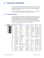
Page 53: ... Row B Row C Row D Row E Row F 25 VCC_5 0E CPCI_REQ64 CPCI_ENUM VCC_3 3E VCC_5 0E GND 24 CPCI_AD 1 VCC_5 0E CPCI_VIO_C24 CPCI_AD 0 CPCI_ACK64 GND 23 VCC_3 3E CPCI_AD 4 CPCI_AD 3 CPCI_5V_D23 CPCI_AD 2 GND 22 CPCI_AD 7 GND CPCI_3V_C22 CPCI_AD 6 CPCI_AD 5 GND 21 VCC_3 3E CPCI_AD 9 CPCI_AD 8 CPCI_M66EN CPCI_CBE 0 GND 20 CPCI_AD 12 GND VCC_VIO CPCI_AD 11 CPCI_AD 10 GND 19 VCC_3 3E CPCI_AD 15 CPCI_AD 14...

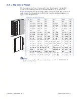
Page 54: ...REQ6 CPCI_GNT6 GND 16 N C N C CPCI_DEG GND N C GND 15 N C GND CPCI_FAL CPCI_REQ5 CPCI_GNT5 GND 14 CPCI_AD 35 CPCI_AD 34 CPCI_AD 33 GND CPCI_AD 32 GND 13 CPCI_AD 38 GND VCC_VIO CPCI_AD 37 CPCI_AD 36 GND 12 CPCI_AD 42 CPCI_AD 41 CPCI_AD 40 GND CPCI_AD 39 GND 11 CPCI_AD 45 GND VCC_VIO CPCI_AD 44 CPCI_AD 43 GND 10 CPCI_AD 49 CPCI_AD 48 CPCI_AD 47 GND CPCI_AD 46 GND 9 CPCI_AD 52 GND VCC_VIO CPCI_AD 51 ...

Page 55: ...ND LPA_BI_DD LPA_BI_DD GND 16 LPB_BI_DA LPB_BI_DA GND LPB_BI_DC LPB_BI_DC GND 15 LPB_BI_DB LPB_BI_DB GND LPB_BI_DD LPB_BI_DD GND 14 GND GND GND GND GND GND 13 SP2_RTS B SP1_RI B SP2_DSR B SP2_DCD B SP2_CTS B GND 12 SP1_RTS B SP2_DTR B VCC_5 0 SP1_CTS B LVDS_BKLTEN GND 11 SP2_TXB SP2_RXB SP1_DTR B SP1_DCD B LVDS_CLKAM GND 10 SP1_TXB SP1_RXB SP1_DSR B SP2_RI B LVDS_CLKAP GND 9 FDC_INDEX FDC_REDWC US...

Page 56: ..._IO 16 GND 18 PMC1_IO 25 PMC1_IO 24 PMC1_IO 23 PMC1_IO 22 PMC1_IO 21 GND 17 PMC1_IO 30 PMC1_IO 29 PMC1_IO 28 PMC1_IO 27 PMC1_IO 26 GND 16 PMC1_IO 35 PMC1_IO 34 PMC1_IO 33 PMC1_IO 32 PMC1_IO 31 GND 15 PMC1_IO 40 PMC1_IO 39 PMC1_IO 38 PMC1_IO 37 PMC1_IO 36 GND 14 PMC_IO 45 PMC1_IO 44 PMC1_IO 43 PMC1_IO 42 PMC1_IO 41 GND 13 PMC1_IO 50 PMC1_IO 49 PMC1_IO 48 PMC1_IO 47 PMC1_IO 46 GND 12 PMC1_IO 55 PMC1...

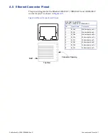
Page 57: ...e A 5 Figure A 5 Ethernet Connector and Pinout ETHERNET CONNECTOR 10BASE T 100BASE TX 1000BASE T PIN Signal Name Description 1 BI_DA Bi directional pair A 2 BI_DA Bi directional pair A 3 BI_DB Bi directional pair B 4 BI_DC Bi directional pair C 5 BI_DC Bi directional pair C 6 BI_DB Bi directional pair B 7 BI_DD Bi directional pair D 8 BI_DD Bi directional pair D Connector Opening Pin 1 Top View ...

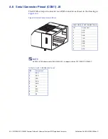
Page 58: ...tor is an RJ45 connector as shown in the drawing in Figure A 6 Figure A 6 Serial Connector and Pinout NOTE An RJ45 to DB9 adapter cable 360 010030 001 is shipped with the CPCI 7806 CPCI 7806RC COM 1 SERIAL PORT CONNECTOR J8 PIN Assignment 1 DCD 2 RTS 3 GND 4 TXD 5 RXD 6 GND 7 CTS 8 DTR Table A 1 RJ45 DB9 Adapter Pinout DB9 Assignment 1 DCD 2 RXD 3 TXD 4 DTR 5 GND 6 NC 7 RTS 8 CTS 9 NC ...

Page 59: ... 2 J21 Connector Pinout PMC Connector J11 J21 PMC Connector J11 J21 Left Side Right Side Left Side Right Side Pin Name Pin Name Pin Name Pin Name 1 GND 2 12V 33 FRAME 34 GND 3 GND 4 INTA 35 GND 36 IRDY 5 INTB 6 INTC 37 DEVSEL 38 5 V 7 BMODE1A 8 5 V 39 PCIXCAP 40 LOCK 9 INTD 10 NC 41 SDONE 42 NC 11 GND 12 NC 43 PAR 44 GND 13 CLK 14 GND 45 VCC_3 3 46 AD 15 15 GND 16 GNT 1 47 AD 12 48 AD 11 17 REQ 18...

Page 60: ...ft Side Right Side Left Side Right Side Pin Name Pin Name Pin Name Pin Name 1 12 V 2 5 V 33 GND 34 NC 3 GND 4 NC 35 TRDY 36 3 3 V 5 5 V 6 GND 37 GND 38 STOP 7 GND 8 NC 39 PERR 40 GND 9 NC 10 NC 41 3 3 V 42 SERR 11 BMODE2 12 3 3 V 43 C BE 1 44 GND 13 RESET 14 GND 45 AD 14 46 AD 13 15 3 3 V 16 GND 47 M66EN 48 AD 10 17 NC 18 GND 49 AD 8 50 3 3 V 19 AD 30 20 AD 29 51 AD 7 52 NC 21 GND 22 AD 26 53 3 3 ...

Page 61: ...CI1_C BE 4 8 GND 39 VCC_3 3 40 PCI1_AD 44 9 VCC_3 3 10 PCI1_PAR64 41 PCI1_AD 43 42 PCI1_AD 42 11 PCI1_AD 63 12 PCI1_AD 62 43 PCI1_AD 41 44 GND 13 PCI1_AD 61 14 GND 45 GND 46 PCI1_AD 40 15 GND 16 PCI1_AD 60 47 PCI1_AD 39 48 PCI1_AD 38 17 PCI1_AD 59 18 PCI1_AD 58 49 PCI1_AD 37 50 GND 19 PCI1_AD 57 20 GND 51 GND 52 PCI1_AD 36 21 VCC_3 3 22 PCI1_AD 56 53 PCI1_AD 35 54 PCI1_AD 34 23 PCI1_AD 55 24 PCI1_...

Page 62: ...42 J14 42 J5 pin D14 11 J14 11 J5 pin E20 12 J14 12 J5 pin D20 43 J14 43 J5 pin C14 44 J14 44 J5 pin B14 13 J14 13 J5 pin C20 14 J14 14 J5 pin B20 45 J14 45 J5 pin A14 46 J14 46 J5 pin E13 15 J14 15 J5 pin A20 16 J14 16 J5 pin E19 47 J14 47 J5 pin D13 48 J14 48 J5 pin C13 17 J14 17 J5 pin D19 18 J14 18 J5 pin C19 49 J14 49 J5 pin B13 50 J14 50 J5 pin A13 19 J14 19 J5 pin B19 20 J14 20 J5 pin A19 5...

Page 63: ...elect a drive device to boot from This feature is useful when installing from a bootable disk For example when installing Windows NT from a CD enter the First Boot menu and use the arrows keys to highlight ATAPI CD ROM Drive Press ENTER to continue with system boot This feature is accessed by pressing the F11 key at the very beginning of the boot cycle The selection made from this screen applies t...

Page 64: ...rts the BIOS revision processor type and clock speed and allows the user to set the system s clock and calendar Use the left and right arrow keys to select other screens Below is a sample of the Main screen The information displayed on your screen will reflect your actual system 002 53 C Copyright 1985 2002 American Megatrends Inc BIOS SETUP UTILITY Main Advanced PCIPnP Boot Security Chipset Exit ...

Page 65: ...se the system to malfunction If problems are noted after changes have been made reboot the system and access the BIOS From the Exit menu select Load Failsafe Defaults and reboot the system If the system failure prevents access to the BIOS screens refer to Chapter One for instructions on clearing the CMOS 002 53 C Copyright 1985 2002 American Megatrends Inc Options shown may not be available on you...

Page 66: ...elow is a sample screen of the PCI PnP menu options in your system may be different from those shown 002 53 C Copyright 1985 2002 American Megatrends Inc BIOS SETUP UTILITY Main Advanced PCIPnP Boot Security Chipset Exit Advanced PCI PnP Settings NO lets the BIOS configure all the devices in the system YES lets the operating system configure Plug and Play PnP devices not required for boot if your ...

Page 67: ...installation Also available in this screen are Boot Settings which allow the user to set how the basic system will act for example support for PS 2 mouse and whether to use Quick Boot or not 002 53 C Copyright 1985 2002 American Megatrends Inc BIOS SETUP UTILITY Main Advanced PCIPnP Boot Security Chipset Exit Boot Settings Configure Settings During System Boot Select Screen Select Item Enter Go to...

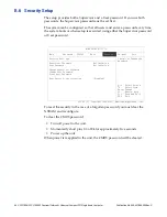
Page 68: ...egatrends Inc To reset the security in the case of a forgotten password you must clear the NVRAM and reconfigure To clear the CMOS password Turn off power to the unit Momentarily short pins 2 3 of E4 for approximately five seconds Power up the unit When power is reapplied to the unit the CMOS password will be cleared BIOS SETUP UTILITY Main Advanced PCIPnP Boot Security Chipset Exit Security Setti...

Page 69: ...d after changes have been made reboot the system and access the BIOS From the Exit menu select Load Failsafe Defaults and reboot the system If the system failure prevents access to the BIOS screens refer to Chapter One for instructions on clearing the CMOS 002 53 C Copyright 1985 2002 American Megatrends Inc BIOS SETUP UTILITY Main Advanced PCIPnP Boot Security Chipset Exit Advanced Chipset Settin...

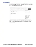
Page 70: ... 2002 American Megatrends Inc If changes have previously been made in the BIOS and the system malfunctions reboot the system and access this screen Select Load Failsafe Defaults and continue the reboot BIOS SETUP UTILITY Main Advanced PCIPnP Boot Security Chipset Exit Exit Options Exit system setup after saving the changes F10 key can be used For this operation Select Screen Select Item Enter Go t...

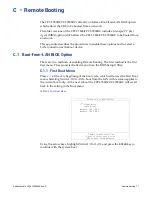
Page 71: ...of enabling Remote Booting The first method is the First Boot menu The second is the Boot menu from the BIOS Setup Utility C 1 1 First Boot Menu Press F11 at the very beginning of the boot cycle which will access the First Boot menu Selecting Network IBA LAN to boot from the LAN in this screen applies to the current boot only At the next reboot the CPCI 7806 CPCI 7806RC will revert back to the set...

Page 72: ...nitializing Intel R Boot Agent Abaco v1 2 40 PXE 2 1 Build 085 WfM2 0 Press Ctrl S to enter Setup Menu Once you press CTRL S the Boot Agent setup menu will appear PXE is the boot option available on the CPCI 7806 CPCI 7806RC You can change the settings for the Setup Prompt and Setup Menu Wait Time You can either enable or disable the prompt and you can set the amount of wait time for the setup men...

Page 73: ...e First Boot menu Selecting Managed PC Boot Agent MBA to boot from the LAN in this screen applies to the current boot only At the next reboot the CPCI 7806 CPCI 7806RC will revert back to the setting in the Boot menu Table C 1 Intel Boot Agent First Boot Menu Using the arrow keys highlight Managed PC Boot Agent MBA and press the ENTER key to continue with the system boot Please select boot device ...

Page 74: ...3 BIOS Features Setup After the Managed PC Boot Agent has been enabled there are several boot options available to the user These options are RPL default TCP IP Netware and PXE The proceeding screen shots show the defaults for each boot method RPL Menu Table C 3 RPL Default Settings BIOS SETUP UTILITY Boot Boot Device Priority Specifies the boot sequence from the available devices Select Screen Se...

Page 75: ...ompt Wait for timeout Boot Failure Next boot device Use cursor keys to edit Up Down change field Left Right change value ESC to quit F9 restore previous settings F10 to save Argon Managed PC Boot Agent MBA v4 00 BIOS Integrated c Copyright 2002 Argon Technology Corporation All rights reserved Configuration Boot Method Netware Protocol 802 3 Config Message Enabled Message Timeout 3 Seconds Boot fai...

Page 76: ...d PC Boot Agent MBA v4 00 BIOS Integrated c Copyright 2002 Argon Technology Corporation All rights reserved Configuration Boot Method PXE Config Message Enabled Message Timeout 3 Seconds Boot Failure Prompt Wait for timeout Boot Failure Next boot device Use cursor keys to edit Up Down change field Left Right change value ESC to quit F9 restore previous settings F10 to save ...

Page 77: ...al are provided in the following section D 1 Microsoft Windows 2000 Professional Software Driver Installation NOTE Prior to installing device drivers Windows 2000 should be updated to Service Pack 4 or later Visit http support microsoft com and search for the latest Service Pack information D 1 1 Video Driver Installation 1 If not already present insert the Windows Drivers CD ROM 2 Click Start Run...

Page 78: ...ction in the right pane of the Computer Management window the driver has not been installed To install the driver right click on the Universal Serial Bus USB controller and select Properties from the drop down menu select the Driver tab and select Update Driver When the wizard starts choose Next and Search for a suitable driver and Next again The Hardware Update Wizard will find the appropriate dr...

Page 79: ...CD ROM 2 Click Start Run Browse In the Look in pull down selection menu select the CD ROM drive Double click on the Hance Rapids folder Double click on the Applications folder Double click on infinst_enu Click OK 3 At the Intel Chipset Software Installation Utility window click Next Click Yes to agree to the software license agreement Click Next At each of the following Hardware Installation windo...

Page 80: ...e right pane D 2 4 Ethernet Adapter Drivers Installation 1 If not already present insert the Windows Drivers CD ROM 2 Click Start right click on My Computer and select Manage In the left pane of the Computer Management window click on Device Manager 3 Intel R PRO 1000 MT Dual Port Server Adapter Perform this step for each of the Ethernet controllers under the Other devices section in the right pan...

Page 81: ...mands E 1 1 Get Device ID This command is used to retrieve the Intelligent device s Hardware Revision Firmware Software Revision and Sensor and Event Interface Command specification revision information 1 Depends on the version of firmware installed on the board 2 Depends on the type of device Table E 1 NetFn 0x06 Cmd 0x01 Byte Value Data Field Comments Request data Response data 1 00 Completion c...

Page 82: ...n code Table E 3 NetFn 0x06 Cmd 0x03 Byte Value Data Field Comments Request data Response data 1 00 Completion code Table E 4 NetFn 0x06 Cmd 0x04 Byte Value Data Field Comments Request data Response data 1 00 Completion code 2 55h 56h 57h 58h FFh All other No error All Self Tests Passed Self Test not implemented in this controller Corrupted or inaccessible data or devices Fatal hardware error Rese...

Page 83: ...used to uniquely identify an instance of a management controller This information can be used in conjunction with the SDR information to verify that a particular controller is still present in the system Table E 5 NetFn 0x06 Cmd 0x06 Byte Value Data Field Comments Request data 1 XXh ACPI System power state The IPMI does not have control over the system power state Therefore this byte is ignored 2 ...

Page 84: ...x08 Byte Value Data Field Comments Request data Response data 1 00h Completion code 2 XXh node 3 XXh node 4 XXh node 5 XXh node 6 XXh node 7 XXh node MS byte 8 XXh clock seq low 9 XXh clock seq high and reserved MS byte 10 XXh time high and version 11 XXh time high and version MS byte 12 XXh time mid 13 XXh time mid MS byte 14 XXh time low 15 XXh time low 16 XXh time low 17 XXh time low MS byte Ta...

Page 85: ...be immediately returned in response to this command Response data 1 XXh Completion code 00h if successful 81h Lost Arbitration 82h Bus Error 83h NAK on Write 84h Truncated Read 2 M Bytes read from the specified slave address Table E 9 NetFn 0x04 Cmd 0x00 Byte Value Data Field Comments Request data 1 XXh Event Receiver Slave Address 0FFh disables Event message generation 7 1 IPMB I2C slave address ...

Page 86: ... says 0xC0 192 decimal the actual voltage is 192 256 3 3 2 5 3 3 3 267 V Table E 11 NetFn 0x04 Cmd 0x2D Byte Value Data Field Comments Request data 1 XXh Sensor Number FFh reserved Response data 1 00h Completion code 2 XXh Sensor reading 3 XXh 7 0b All event messages disabled for this sensor 6 0b Sensor scanning disabled 5 1b Initial update in progress 4 0 reserved 4 XXh For threshold based sensor...

Page 87: ...nd is used to obtain information about the size and access method of the FRU Inventory data in the device E 3 11 Read FRU Data This command returns the specified data from the FRU Inventory Info area No parsing of the FRU data is performed by the IPMI subsystem system management software is responsible for interpreting the FRU data Table E 12 NetFn 0x0A Cmd 0x10 Byte Value Data Field Comments Requ...

Page 88: ... structures and writing the data to the FRU area Table E 13 NetFn 0x0A Cmd 0x11 Byte Value Data Field Comments Request data 1 XXh FRU device ID FFh reserved 2 XXh FRU Inventory offset to read LS Byte 3 XXh FRU Inventory offset to read MS Byte Offset is in words or bytes per device access type returned in the FRU Inventory Area Info command 4 XXh Count to read 1 based Response data 1 00 Completion ...

Page 89: ...ommand returns the Record Header for the first SDR in the repository FFFFh specifies that the last SDR in the repository should be listed If Record ID is non zero the command returns the information from the matching record and the Record ID for the next SDR in the repository Table E 15 NetFn 0x0A Cmd 0x20 Byte Value Data Field Comments Request data Response data 1 00h Completion code 2 51h SDR Ve...

Page 90: ... 00 00 00 00 00 00 00 00 00 00 00 0060 00 00 00 00 00 00 00 00 00 00 00 00 00 00 00 00 0070 00 00 00 00 00 00 00 00 00 00 00 00 00 00 00 00 0080 00 00 00 00 00 00 00 00 00 00 00 00 00 00 00 00 0090 00 00 00 00 00 00 00 00 00 00 00 00 00 00 00 00 00A0 00 00 00 00 00 00 00 00 00 00 00 00 00 00 00 00 00B0 00 00 00 00 00 00 00 00 00 00 00 00 00 00 00 00 00C0 00 00 00 00 00 00 00 00 00 00 00 00 00 00 0...

Page 91: ... For IPMB messages this field is equated to the Requestor s Slave Address and LUN fields Thus the Generator ID information is not carried in the data field of an IPMB request message Table E 18 NetFn 0x04 Cmd 0x02 Byte Value Data Field Comments Request data Generator ID RqSA RqLun 1 03h EvMRev IPMB v 1 0 message 2 XXh Sensor Type 02h voltage sensors 01h temperature sensors 3 XXh Sensor Sensor numb...

Page 92: ...06RC E 7 1 IPMB Relay This command allows the CPCI 7806 CPCI 7806RC connected to the Zircon s I2 C1 bus to have the Zircon send a command on its I2 C0 bus which is connected to the IPMB pins on the backplane and for the Zircon to send the response to that command back to the CPCI 7806 CPCI 7806RC on I2C1 NOTE The Zircon will accept an IPMB Relay request on its I2 C0 bus but it will always send the...

Page 93: ... first CPCI 7806 CPCI 7806RC 6e 14 7e ba 00 2d 00 1e c0 c0 00 7b Note that the first CPCI 7806 CPCI 7806RC does not receive a response which has the NetFn and Cmd for IPMB Relay but rather the successful request System management software that will use the IPMB Relay function must anticipate that the NetFn Cmd and RsSA will match the values in the IPMB Relay request data payload not the header As ...

Page 94: ...r to the originating device as the Zircon has already responded Software on the CPCI 7806 CPCI 7806RC should set the forwarding address first then use IPMB relay to send a Set Event Receiver command to the alarm cards or other IPMI devices in the chassis E 7 3 Set Platform Event Forwarding Address This command sets the slave address and the LUN of the Event Receiver to which the Platform Events ar...

Page 95: ...DED AS IS WITH NO REPRESENTATIONS OR WARRANTIES OF ANY KIND WHETHER EXPRESS OR IMPLIED INCLUDING BUT NOT LIMITED TO WARRANTIES OF DESIGN MERCHANTABILITY OR FITNESS FOR A PARTICULAR PURPOSE ALL OTHER LIABILITY ARISING FROM RELIANCE ON ANY INFORMATION CONTAINED HEREIN IS EXPRESSLY DISCLAIMED Abaco Systems Information Centers Americas 1 866 652 2226 866 OK ABACO or 1 256 880 0444 International Europe...

Reviews: