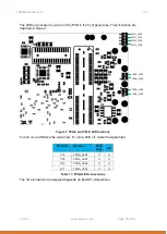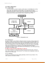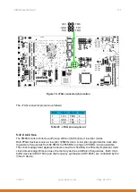
FM680 User Manual
r1.7
FM680
Page 21 of 32
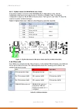
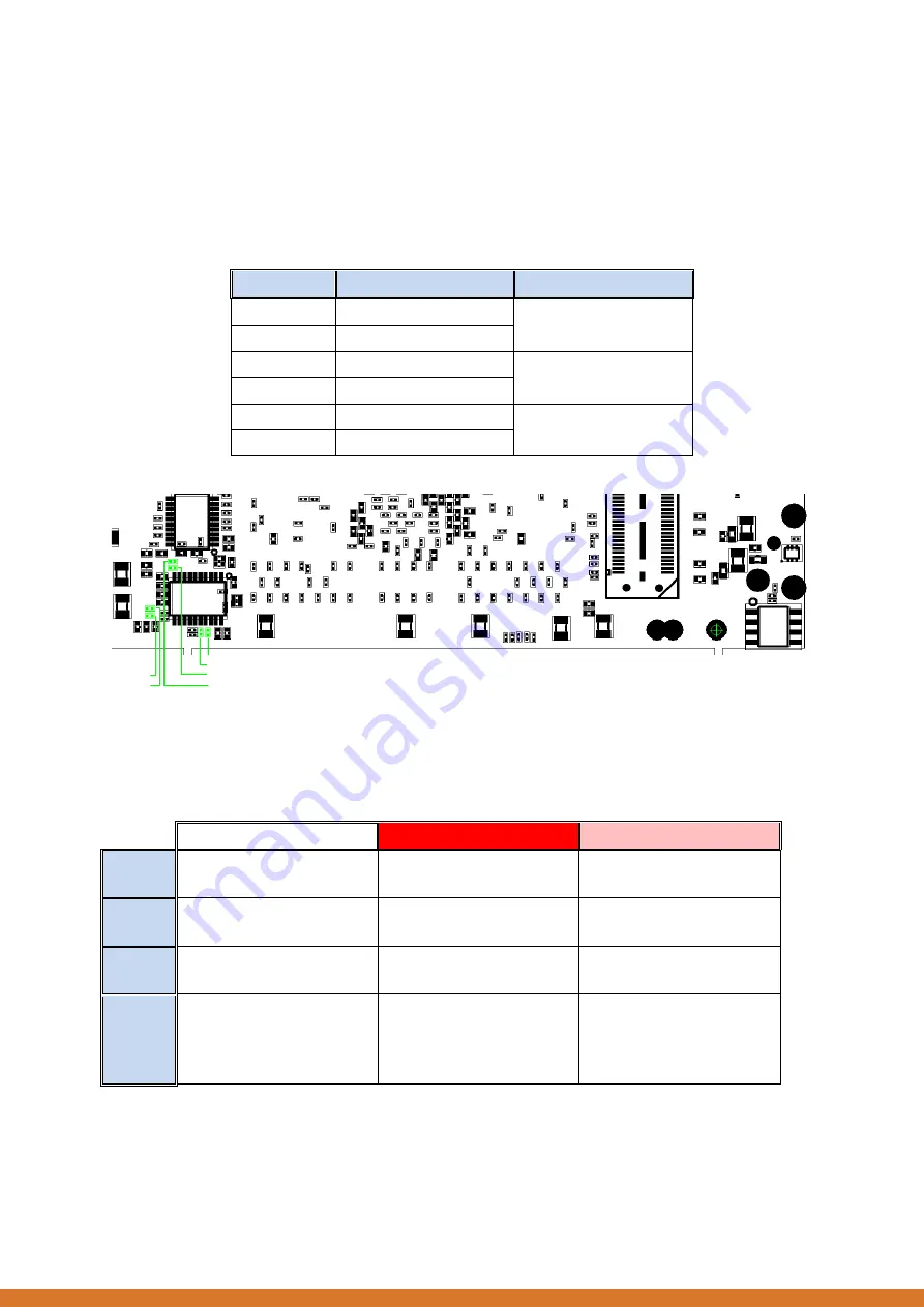
5.9.4 Optical transceiver MGT Reference Clock
A low jitter oscillator connects to the 874003BG-05LF. Depending on the resistor
configuration this device can output a 312.5, 156.25 or 125 MHz clock. The default
configuration outputs a 156.25 MHz reference clock. The Figure 6 and Table 15 show the
selection resistor locations and type.
Table 15: Optical transceiver reference clock frequency selection resistors
Resistor
Type
MGT REFCLK
R510
Pull up
(default)
FSEL0
R518
Pull down
R294
Pull up
(default)
FSEL1
R494
Pull down
R292
Pull up
(default)
FSEL2
R293
Pull down
518
510
R294
R494
R292
R293
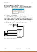
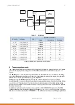
Figure 6: Optical transceiver reference clock selection resistors locations
5.10 FPGA LED
Four LEDs are connected to the Virtex-5 device. In the default FPGA firmware, the LEDs are
driven by the Virtex-5 device. The following table shows the meaning of the LEDs in the
standard reference design.
OFF
ON
FLASHING
LED 0
(red)
PCIexpresslink down
PCIexpress link up
n.a.
LED 1
(red)
No PCI express traffic
PCI express traffic
PCI express traffic
LED 2
(red)
No PCI express traffic
PCI express traffic
PCI express traffic
LED 3
(red)
FM680 PCB revision 2
FM680 PCB revision 1
(only when FPGA A
firmware revision is 2.3
or higher)
n.a.
Table 16: LED board status


