background image

58 SBC347A 3U VPX Single Board Computer

Publication No. 500-9300527837-000 Rev. A.0

5.21 FPGA

The FPGA is a Microsemi SmartFusion2 device that provides the following 
facilities:

• Board Configuration, Control and Status registers

• Three UARTs (COM1 to COM3)

• Watchdog timer

• GPIO  controller

• General purpose timers

• NVRAM  interface

• Reset  control

• Ancillary logic functions

• AXIS support

LINK

For more details on the FPGA device, see 

http://www.microsemi.com

.

5.21.1 Registers

See 

Section 6 •

ʺ

FPGA Registers

ʺ

 on 

page 60

.

5.21.2 AXIS Support

AXIS is a set of software modules that can be used to accelerate the design, 
development, testing, and deployment of complex digital signal processor (DSP) 
and multiprocessing platforms for real-time applications such as radar, sonar, 
communications, and image processing.

AXIS requires two external hardware signals (AXIS_CLK and AXIS_RST) to allow 
boards to synchronize over the backplane while running AXIS software.

On the SBC347A, these signals are shared with GPIO(2) and GPIO(3), 
respectively. For AXIS to be fully supported, these signals must be available (i.e., 
the build variant must be SBC347A-xxxx1xxx). Also, these signals must not be 
connected to any external loads that can interfere with their operation.

See 

Section 6.13

ʺ

AXIS Timestamp Registers (0x648 to 0x64D)

ʺ

 on 

page 64

 for 

information on the AXIS timestamp registers.

Summary of Contents for SBC347A-11330001

Page 1: ... Manual SBC347A 3U VPX Single Board Computer THE SBC347A IS DESIGNED TO MEET THE EUROPEAN UNION EU RESTRICTIONS OF HAZARDOUS SUBSTANCE RoHS DIRECTIVE 2002 95 EC CURRENT REVISION Publication No 500 9300527837 000 Rev A 0 ...

Page 2: ...inal Release Abaco Systems is registered with an approved Producer Compliance Scheme PCS and subject to suitable contractual arrangements being in place will ensure WEEE is processed in accordance with the requirements of the WEEE Directive Abaco Systems will evaluate requests to take back products purchased by our customers before August 13 2005 on a case by case basis A WEEE management fee may a...

Page 3: ...e a D subscript and binary numbers have a b subscript The prefix 0x shows a hexadecimal number following the C programming language convention Thus One dozen 12D 0x0C 1100b The multipliers k M and G have their conventional scientific and engineering meanings of x103 x106 and x109 respectively and can be used to define a transfer rate The only exception to this is in the description of the size of ...

Page 4: ...ible to include all the detailed data on all such devices in this manual A list of the specifications and data sheets that provide additional information follows These are the latest versions at time of writing check associated websites for later updates NOTE Registration may be required for access to these specifications LINKS http www vita com http www ieee org http www pcisig org NOTE Technical...

Page 5: ...ry in the Technical Support database and allocate it a unique Case number for use in any future correspondence Alternatively you may also contact Abaco s Technical Support via LINK support abaco com Returns If you need to return a product there is a Return Materials Authorization RMA form available via the website Embedded Support page LINK https www abaco com embedded support Do not return produc...

Page 6: ...nd Power Up Reset 21 4 1 Power Supply Requirements 21 4 2 Board Keying 21 4 3 Board Installation Notes 22 4 4 Connecting to SBC347A 23 4 4 1 Rear Transition Module 23 4 5 Reset and Power up Sequence 24 4 6 BIOS Setup Utility 24 4 6 1 Accessing the Setup Menus 24 4 7 First Boot Menu 25 4 8 About the Setup Menus 26 4 9 Main Menu 27 4 10 Advanced Menu 28 4 11 Chipset Menu 29 4 12 Security Menu 30 4 1...

Page 7: ... 50 5 15 2 Board Temperature Sensor 50 5 15 3 CPU Die Temperature Sensor 50 5 16 Timers 51 5 16 1 General Purpose Timers 51 5 16 2 Watchdog Timer 51 5 17 Power Sequencing 52 5 17 1 Onboard Sequencing 52 5 17 2 Inter board Sequencing 52 5 18 LEDs 53 5 18 1 BIT LEDs DS401 to DS404 54 5 18 2 Board Reset LED DS405 54 5 18 3 Sleep Status LED DS406 55 5 18 4 Board Power Good LED DS407 55 5 18 5 SSD Acti...

Page 8: ...RQ Clear Register 0x65A 66 6 19 Timer 0 Data Bytes 0 to 3 Registers 0x654 to 0x657 66 6 19 1 Reads 66 6 19 2 Writes 67 6 20 Timer 1 Data Bytes 0 to 3 Registers 0x65C to 0x65F 67 6 20 1 Reads 67 6 20 2 Writes 67 6 21 GPIO Out Register 0x670 67 6 22 GPIO In Register 0x671 68 6 23 GPIO Direction Register 0x672 68 6 24 GPIO Interrupt Enable Register 0x673 68 6 25 GPIO Level Edge Register 0x674 68 6 26...

Page 9: ... Erase Control Register 0x6BF 78 6 63 SSD Cache Flush Control Register 0x6C0 78 6 64 VPX Control Register 0x6C1 78 6 65 Scratchpad Register 0x6C6 78 6 66 Test Register 0x6C7 79 6 67 Backplane Status Register 0x6CA 79 6 68 SSD Status Register 0x6CB 79 6 69 Write Protection Status Register 0x6CC 80 6 70 Board Jumper Link Status Register 0x6CD 80 6 71 Boot Location Status Register 0x6CE 81 7 Connecto...

Page 10: ...ion cooled Boards 99 A 6 Product Codes 100 A 7 Software Support 101 A 7 1 BIOS 101 A 7 2 Built In Test 101 A 7 3 Background Condition Screening 101 A 8 I O Modules 102 B Statement of Volatility 103 B 1 Volatile Memory 103 B 2 Nonvolatile Memory 104 C Thermal Derating 105 C 1 Processor Option 1 Quad Core 105 Glossary 106 Index 108 ...

Page 11: ...gure 4 7 Save Exit Menu 32 Figure 4 8 Event Logs Menu 33 Figure 5 1 Block Diagram 34 Figure 5 2 Additional PCIe Connectivity 39 Figure 5 3 RS422 RS485 Signal Definition 42 Figure 5 4 I2C Bus Structure 47 Figure 5 5 Onboard Sensor and System Management Bus Architecture 49 Figure 5 6 Rear LED Positions 53 Figure 5 7 JTAG Chains 56 Figure 5 8 Air cooled Front Panel 59 Figure 5 9 Conduction cooled Fro...

Page 12: ... 53 Table 5 16 BIT LED Meanings 54 Table 5 17 BIT Status LED Meanings 54 Table 5 18 Power States 55 Table 5 19 Reset Sources 57 Table 6 1 FPGA Registers 60 Table 7 1 Connector Functions 82 Table 7 2 P0 Pin Assignments 83 Table 7 3 J0 Pin Assignments 83 Table 7 4 P1 Pin Assignments 84 Table 7 5 J1 Pin Assignments 85 Table 7 6 P2 Pin Assignments 86 Table 7 7 J2 Pin Assignments 87 Table 7 8 P1 Pin As...

Page 13: ...Tables 13 Table A 11 Conduction cooled Environmental Specifications 99 Table A 12 Product Options 100 Table B 1 Volatile Memory 103 Table B 2 Nonvolatile Memory 104 Table C 1 Maximum Processor Speed versus Maximum Temperature for Processor Option 1 105 ...

Page 14: ...terfaces including 10GBASE T Ethernet 10 GbE USB SATA and General Purpose Input Output GPIO The Core i7 processor also provides a DDR3 SDRAM interface with error checking and correction ECC An Intel Series 8 peripheral controller hub PCH bridge provides three SATA interfaces four USB ports a low pin count LPC bus and a Serial Peripheral Interface SPI supporting SPI boot Flash The SBC347A also prov...

Page 15: ...e optional DVI video port Two serial COM ports Up to four channels of USB 2 0 connectivity to the VPX backplane Up to three SATA channels connected to the VPX backplane Up to 14 lanes of PCI Express one x8 one optional x4 and optional x2 to the VPX backplane Up to eight bits of General Purpose I O with interrupt capability Elapsed time indicator Watchdog timers Ambient and chip temperature sensors...

Page 16: ... rack enclosure to an electrical ground If AC power is supplied to the rack enclosure the power jack and mating plug of the power cable must meet IEC safety standards 1 2 1 Flammability The SBC347A circuit board is made by a UL recognized manufacturer and has a flammability rating of UL94V 1 1 2 2 EMI EMC Regulatory Compliance CAUTION This equipment generates uses and can radiate electromagnetic e...

Page 17: ... the heatsink There are no user alterable components underneath the heatsink so users should have no reason to remove it Users should not attempt reattachment of the heatsink as this requires precise torque on the screws attaching the heatsink to the PCB Over tightening the screws may cause the heatsink to damage components beneath it Removal and re attachment of the heatsink should only be carrie...

Page 18: ...tion product code product description equipment number and board revision Figure 2 1 Product Label Packaging 2 2 Inspection When handling the SBC347A observe antistatic precautions Visually examine the SBC347A for any physical damage If the SBC347A is not received in perfect physical condition report this to Abaco s Technical Support immediately See ʺTechnical Support Contact Informationʺ on page ...

Page 19: ...he standard kit of parts additional jumpers may be obtained on request These are suitable for level 1 to 3 low vibration applications Figure 3 1 Link Positions The diagram above shows standard 2 54 mm pitch headers for general use This manual refers to jumper settings as In or Out Meanings are as follows In jumper fitted Out jumper not fitted ...

Page 20: ...overy device is for use if the Main device is corrupted Booting from the Recovery device puts the SBC347A into Recovery mode Here onboard configuration EEPROMs are disabled allowing devices to come up using default strapping 3 3 2 Configuration EEPROM Write Enable Link P4 Nonvolatile configuration EEPROM devices on the board are used to configure the initial state of the PCIe switch and memory ser...

Page 21: ...ts are as follows The VBAT supply may be used to power the Real Time Clock RTC in isolation when the board is powered down to maintain the time date information This requires up to 6 µA at 3 3 V 5 See Section A 2 ʺElectrical Specificationʺ on page 96 for more details 4 2 Board Keying The keying pins are used to define slot specific keying The SBC347A is delivered with module keying devices of the ...

Page 22: ...ews at the top and bottom of the front panel allow the board to be tightly secured in position which provides continuity with the chassis ground of the system 3 Conduction cooled versions of the SBC347A have screw driven wedgelocks to provide the necessary mechanical thermal interface Correct adjustment requires a calibrated torque wrench with a hexagonal head of size 3 32 2 38 mm set to between 0...

Page 23: ...pins using a Rear Transition Module RTM COM1 is configured as Data Terminal Equipment DTE with default settings of 115200 baud 8 bits character 1 stop bit parity disabled and no flow control 4 4 1 Rear Transition Module For development systems connection to the board I O can be achieved using an RTM This converts the condensed pinout of the backplane connectors to pinouts suitable for use by indus...

Page 24: ...eep Status LED DS406 is lit when the SBC347A is in a sleep state S3 to S5 The SBC347A supports the SEQ_IN SEQ_OUT power sequencing signals on the P2 connector pins G13 and G15 in line with other Abaco boards When connected in a power sequencing daisy chain the onboard power supplies will only power up when SEQ_IN is asserted or floating high See Section 5 17 2 ʺInter board Sequencingʺ on page 52 f...

Page 25: ...enter this menu and use the arrows keys to highlight ATAPI CD ROM Drive Press ENTER to continue with the boot The First Boot menu is accessed by pressing the F7 key at the very beginning of the boot cycle The selection made from this screen applies to the current boot only and will not be used during the next boot up of the SBC347A If you have trouble accessing the First Boot menu from the Boot me...

Page 26: ...ption or sub menu then press Enter to pick that sub menu or option for altering To step through the range of available settings e g enabled disabled for that option use the and keys When in a sub menu the Setup menu selection line shows the top level menu selection only This section shows examples from a working SBC347A While the general type and level of information displayed should be similar fo...

Page 27: ...wn on entry to Setup It reports details on the BIOS firmware the board and the processor It also allows the user to set the System Language English is the default and currently the only option and the SBC347A clock calendar although without battery backup any power cycle will reset the clock Figure 4 2 Main Menu ...

Page 28: ...nd chipset settings CAUTION Changes made from some menus can cause the SBC347A to malfunction If problems are detected after changes have been made reboot the board and access the Setup Select the Save Exit menu pick Restore Defaults then save these changes and reboot the board e g by picking Save Changes and Reset Figure 4 3 Advanced Menu ...

Page 29: ...settings for the chipsets are processor dependent take care when changing settings from the defaults set at the factory CAUTION Changes made from some menus can cause the SBC347A to malfunction If problems are detected after changes have been made reboot the board and access the Setup Select the Save Exit menu pick Restore Defaults then save these changes and reboot the board e g by picking Save C...

Page 30: ...use of these passwords If both passwords are to be used the Administrator password must be set first Figure 4 5 Security Menu CAUTION Take care when setting passwords Once a password is set there is no method available to the user to reset it without using that original password If a password is lost the BIOS will need to be reprogrammed Should this event occur contact technical support for assist...

Page 31: ... booting from a remote network The devices shown in this menu are the bootable devices detected during POST If an installed drive does not appear verify the hardware installation Also available in this menu are Boot Configuration settings that allow the user to set how the SBC347A acts for example whether to use ʹFast Bootʹ Figure 4 6 Boot Menu ...

Page 32: ...des options on saving Setup selections and exiting Setup Figure 4 7 Save Exit Menu If changes have previously been made from the Setup menus and the SBC347A malfunctions reboot the board and select this screen Pick Restore Defaults then save these changes and reboot the board e g by picking Save Changes and Reset ...

Page 33: ...lication No 500 9300527837 000 Rev A 0 Installation and Power Up Reset 33 4 15 Event Logs Menu This menu provides option of changing settings of event logs or viewing event logs Figure 4 8 Event Logs Menu ...

Page 34: ...essed only through mechanisms provided by the Operating System s Board Support Package and not directly by application software If a standard operating system is not being used then it is recommended that applications are written in such a way as to minimize direct access to hardware resources bearing in mind that changes may be necessary to support future iterations of the hardware Abaco supporte...

Page 35: ...Integrated Graphics controller GT2 The following table shows the Processor Stock Keep Units SKUs supported Contact your nearest Abaco sales office or agent for the latest processor options and speeds NOTE The CPU operating frequency and the temperature are inter dependent This means that for a given temperature a maximum CPU operating frequency is achievable and conversely for a given CPU operatin...

Page 36: ...ollowing table shows supported RAM configurations The RAM operates at an interface speed of 1600 megatransfers second NOTE The actual RAM configuration fitted to the SBC347A may change as different RAM density devices become available Check with the factory for latest memory capability 5 2 2 Boot Flash The SBC347A has a total of three 16 MByte SPI Flash devices fitted for Management Engine ME BIOS...

Page 37: ...status along with the SSD presence from the FPGA The FPGA also provides a Fast Erase facility See relevant software documentation for information on how to activate this function 5 2 4 NVRAM A 512 KByte Cypress FM22LD16 Ferro electric Random Access Memory FRAM device provides memory mapped nonvolatile memory on the SBC347A This device is write protected by bits in the EEPROM DIP switch which can b...

Page 38: ...is capable of 10GBASE T operation 5 3 2 Module Maskable Reset OpenVPX supports a second reset input from the backplane P1 pin G15 which may be masked under software control The SBC347A is hard reset when the Maskable Reset backplane signal is asserted for more than 10 µS unless masked by software in the FPGA The reset is not masked by default The SBC347A is also able to drive the Maskable Reset un...

Page 39: ...gure 5 2 Additional PCIe Connectivity NOTE Optional x2 and x4 PCIe ports from the PCH are only available when I O product option 1 5 5 1 PCI Express Gen3 Operation The SBC347A PEG port lanes are compatible with PCIe Gen3 operation across the backplane The ability to operate at Gen3 depends on the physical parameters of the complete channel i e the backplane the SBC347A and the link partner so Gen3...

Page 40: ...H0 and ETH1 are provided by the Intel X540 Controller The interface supports 10 100 1000 10GBASE T auto negotiation automatic Musical Instrument Digital Interface MIDI crossover and polarity NOTE User may experience dropped Ethernet packets during cold start below 25 C or during thermal transition 5 6 1 Dual 10GBASE T Table 5 3 ETH0 ETH1 Pin Mapping Dual BASE T Variant Signal P1 Pin Signal P1 Pin ...

Page 41: ... configured accordingly 5 8 Serial Ports The SBC347A provides a total of three serial COM ports of which two COM1 and COM2 are available to the user The third port is connected to the optional onboard Intelligent Platform Management Interface IPMI Board Management Microcontroller BMM The COM ports each have a 16C550 universal asynchronous receiver transmitter UART compatible register set and suppo...

Page 42: ...lternatively when in RS422 mode software must set the Ready to Send RTS signal high by writing to the appropriate UART register to enable the transceiver Again this configuration is accessible in the BIOS set up screen CAUTION Take care when connecting RS422 RS485 receivers to either COM port The default mode of operation is RS232 which could cause damage to an RS422 RS485 receiver because of its ...

Page 43: ... O product option 1 All backplane ports are capable of operating at SATA Revision 3 0 data transfer rates up to 6 Gbit s NOTE Due to limitations in the VPX backplane bandwidth capability the use of signal redrivers at the system level may be required to guarantee SATA 6 Gbit s operation The SBC346ARTM includes redrivers on the SATA ports A single LED DS413 on the rear of the printed wiring board P...

Page 44: ...ured as inputs with the ability to generate level or edge triggered interrupts The GPIO signals are intended only to be used by Abaco software drivers See the relevant software manual for details GPIO 2 and GPIO 3 are shared with the AXIS_CLK and AXIS_RST signals respectively If Advanced Multiprocessor Integrated Software AXIS operation is required these signals cannot be used as GPIO See Section ...

Page 45: ...ion is provided on all video signals LINK For more information on the integrated Graphics Controller see http www Intel com 5 11 2 DVI The SBC347A provides an optional Digital Visual Interface DVI port on the VPX backplane connector Resolutions up to 1920x1200 may be supported The DVI is only available when the I O product option 1 Table 5 9 VGA Signal Availability Signal P2 Pin VGA_RED A15 VGA_GR...

Page 46: ...nerate 2048 bit Rivest Shamir and Adleman RSA keys in 500 ms 5 13 Real Time Clock The PCH provides an RTC powered from the P3V3_AUX or the VBAT supply When either of these supplies is present the system clock is maintained if all power is removed the RTC is reset The RTC module comprises a clock with 1 second resolution two banks of static RAM and the following interrupt features Time of day alarm...

Page 47: ...amount of time for which the SBC347A has been powered and the number of power cycles Powerup time is only recorded when the platform is fully powered and not in S3 S4 or S5 states Power cycle events are only recorded when the backplane VS3 5V power rail transitions from on to off The ETI is intended only to be used by Abaco software drivers See the relevant software manual for details LINK For mor...

Page 48: ...allows the BIOS to use standard routines to detect and configure the memory during boot up This device is only write enabled when a jumper is fitted on the Configuration EEPROM Write Enable Link P4 see page 20 or when the appropriate bit in the EEPROM DIP switch is set see above and when the backplane NVMRO signal on P0 pin A4 is inactive Table 5 12 DIP Switch Options Output Datasheet Name Functio...

Page 49: ...rt number and serial number The BMM can reset or power off the SBC347A in response to a System Management request The BMM can control the state of the BIT Fail LED DS401 to indicate BIT status The following diagram shows the onboard sensor and System Management bus architecture Figure 5 5 Onboard Sensor and System Management Bus Architecture The onboard sensors can be accessed at the following add...

Page 50: ...S3 S4 or S5 sleep state See Section 5 18 ʺLEDsʺ on page 53 5 15 2 Board Temperature Sensor An LM92 digital temperature sensor monitors the ambient temperature on the printed circuit board PCB and can be used by system health monitoring software either on the SBC347A or on an external IPMI controller to determine the ambient operating temperature of the board The sensor has an accuracy of 0 33 C LI...

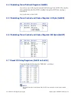
Page 51: ...as a start value The timers can be programmed to roll over on expiry and reload the initial start value or they can be programmed into one shot mode where they will stop counting when expired Together these features provide a highly flexible timer solution The FPGA timers are intended only to be used by Abaco software drivers See the relevant software manual for details 5 16 2 Watchdog Timer The F...

Page 52: ...er Manager will shut down all onboard supplies except P3V3_AUX 5 17 2 Inter board Sequencing The SBC347A supports a proprietary inter board power sequencing mechanism This allows for the sequencing of power between several boards in a system to be controlled limiting overall inrush current and is achieved via the SEQ_OUT and SEQ_IN signals on the P2 connector which can be daisy chained between boa...

Page 53: ... daisy chain is broken DS406 Sleep status Yellow The board is in sleep state S3 S4 or S5 DS407 Power OK Green All backplane and onboard supplies are within specification Also used with DS406 to indicate the sleep status DS408 SSD activity Yellow The SSD device is active DS413 SATA activity Green Any of the PCH SATA ports are active DS414 to DS421 POST status Yellow Shows the value of the most rece...

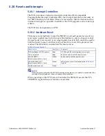
Page 54: ... signal is driven active low using an open drain driver when the red LED is lit When BIT is not installed on the SBC347A other OSs may use the BIT status LEDs to indicate status See the relevant software manual for more information 5 18 2 Board Reset LED DS405 The platform reset signal drives this red LED to show that the SBC347A is in reset There are several reset sources that could cause the pla...

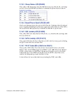
Page 55: ...he drive is being read from or written to 5 18 6 SATA Activity LED DS413 This green LED when lit shows that there is SATA activity on any port including the port connected to the onboard SSD 5 18 7 POST Code LEDs DS414 to DS421 These yellow LEDs reflect the value of most recent port 80 write cycle where DS414 bit 0 of the PORT80 register and DS421 bit 7 BIOS Power On Self Test POST writes values t...

Page 56: ...r Debug Port The SBC347A provides access to the debug port on the processor via the TAC This includes a Samtec 60 way SH 030 01 L D A connector in accordance with Intel recommendations and conforms to the Intel eXtended Debug Port XDP standard pinout allowing probes from various vendors to be used A TAC is available if required part number SBC326TST 11 Contact Abaco for ordering information JTAG H...

Page 57: ... reset which cannot be used to hold the board in reset and they may not result in a reset if the processor has crashed The table below summarizes the reset sources NOTE Global type resets will result in the SBC347A entering a sleep state so it is normal to see onboard LEDs switching off accordingly and it does not indicate a fault condition When operating as the VPX System Controller the SBC347A a...

Page 58: ...sed to accelerate the design development testing and deployment of complex digital signal processor DSP and multiprocessing platforms for real time applications such as radar sonar communications and image processing AXIS requires two external hardware signals AXIS_CLK and AXIS_RST to allow boards to synchronize over the backplane while running AXIS software On the SBC347A these signals are shared...

Page 59: ...A 0 Functional Description 59 5 22 Front Panel 5 22 1 Air cooled Versions Build Levels 1 to 3 Figure 5 8 Air cooled Front Panel 5 22 2 Conduction cooled Versions Build Levels 4 and 5 Figure 5 9 Conduction cooled Front Panel VITA 48 1 Pitch ...

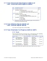
Page 60: ...8 Reserved 0x685 to 0x687 Reserved 0x629 BIT C S Read Write 0x688 VPX GDISCRETE1 Out Read Write 0x62A to 0x634 Reserved 0x689 VPX GDISCRETE1 In Read Write 0x635 NVRAM Memory Space Page Read Write 0x68A VPX GDISCRETE1 Direction Read Write 0x636 to 0x647 Reserved 0x68B VPX GDISCRETE1 Interrupt Enable Read Write 0x648 to 0x64D AXIS Timestamp 0 to 5 Read only 0x68C VPX GDISCRETE1 Level Edge Read Write...

Page 61: ...d Write 0x6AD Ancillary Audio Availability Read only 0x6C1 VPX Control Read Write 0x6AE Front Panel Configuration Read only 0x6C2 to 0x6C5 Reserved 0x6AF and 0x6B0 Reserved 0x6C6 Scratchpad Read Write 0x6B1 SSD Availability Read only 0x6C7 Test Read only 0x6B2 SSD Secure Hardware Erase Capability Read only 0x6C8 and 0x6C9 Reserved 0x6B3 to 0x6B7 Reserved 0x6CA Backplane Status Read only 0x6B8 UART...

Page 62: ...ters 0x610 to 0x61A These read back ASCII values for SBC347A as follows NOTE Code should be written to read bytes until the first NULL is encountered or the last byte is reached 0x61A Bits Read Write Description Default 7 to 1 Read only Reserved 0000000b 0 Read Write WDT enable 1 WDT enabled 0 WDT disabled 0b Bits Read Write Description Default 7 to 3 Read only Reserved 00000b 2 to 0 Read Write WD...

Page 63: ...6 Read onlya a It is not possible to control the BIT Fail LED directly control is only possible via the BMM BIT Fail LED DS401 0 5 Read Write BIT Status 1 LED DS402 1 LED lit 0 LED not lit 0 sticky on BIT reset 4 Read Write BIT Status 2 LED DS403 1 LED lit 0 LED not lit 0 sticky on BIT reset 3 to 0 Read only Reserved 0000b Bits Read Write Description Default 7 Read Write Select the other boot devi...

Page 64: ...eviously run 01 Fast BIT performed 10 Full BIT performed 11 Fast Start performed 00b sticky when reset using HRESET request 4 Read Write BIT pass fail 1 BIT failed 0 BIT passed 1 sticky when reset using HRESET request 3 Read Write Fast BIT 1 Fast BIT enabled via BIOS setting 0 Fast BIT disabled 0 2 Read Write Fast Start 1 Fast Start enabled via BIOS setting 0 Fast Start disabled 0 1 Read only Rese...

Page 65: ...utputs inhibited 0 Do not drive clock onto GPIO2 GPIO2 and GPIO3 behave as GPIO signals 0 6 Read Write AXIS reset signal 1 Assert AXIS reset signal on GPIO3 0 De assert AXIS reset signal on GPIO3 This bit is only functional when bit 7 is set N A 5 to 0 Read only Reserved 000000b Bits Read Write Description Default 7 Read only Timer IRQ status 1 Pending 0 No interrupt N A 6 Read only Reserved 0 5 a...

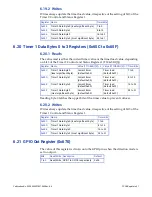
Page 66: ...1 Latch all timers on read of timer 0 LSBa 0 Latch individual timers on read of individual timer LSB a Setting this bit in either timer Control and Status Register 2 latches all timers on a read of the timer least significant byte 0 3 and 2 Read only Reserved 00b 1 Read Write Timer one shot enable 1 Timer will count down and stop 0 Timer will count down and reload at terminal count 0 0 Read Write ...

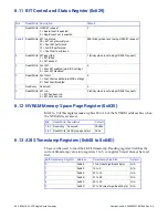
Page 67: ...t Register Name Timer Bits 0x654 Timer 0 Data Byte 0 least significant byte 7 to 0 0x655 Timer 0 Data Byte 1 8 to 15 0x656 Timer 0 Data Byte 2 16 to 23 0x657 Timer 0 Data Byte 3 most significant byte 24 to 31 Register Name Value if T1C SR1 3 0 Value if T1C SR1 3 1 Timer Bits 0x65C Timer 1 Data Byte 0 least significant byte Current timer default 0x00 Timer load default 0xFF 7 to 0 0x65D Timer 1 Dat...

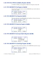
Page 68: ... pin active high low or rising falling edge depending on the sensitivity mode Bits Read Write Description Default 7 to 0 Read Write GPIO7 to GPIO0 respectively 0x00 Bits Read Write Description Default 7 to 0 Read Write GPIO7 to GPIO0 respectively 1 Output 0 Input 0x00 Bits Read Write Description Default 7 to 0 Read Write GPIO7 to GPIO0 respectively 1 Interrupt enabled 0 Interrupt masked 0x00 Bits ...

Page 69: ...ead Write Description Default 7 to 0 Read Write GPIO7 to GPIO0 respectively 1 Both edge mode enabled 0 Both edge mode disabled 0x00 Bits Read Write Description Default 7 to 0 Read Write GPIO7 to GPIO0 respectively 1 Interrupt pending 0 No interrupt 0x00 Bit Description Default 7 GPIO7 availability 1 GPIO7 available 0 GPIO7 not available N A 6 GPIO6 availability 1 GPIO6 available 0 GPIO6 not availa...

Page 70: ...ETE1 Interrupt Enable Register 0x68B 6 35 VPX GDISCRETE1 Level Edge Register 0x68C This sets the interrupt detection sensitivity of the GDISCRETE1 pin level or edge mode Bits Read Write Description Default 7 Read Write GDISCRETE1 0 6 to 0 Read only Reserved 0000000b Bits Read Write Description Default 7 Read Write GDISCRETE1 0 6 to 0 Read only Reserved 0000000b Bits Read Write Description Default ...

Page 71: ...1 to bit 7 to clear the interrupt 6 39 VPX GDISCRETE1 Availability Register 0x690 Bits Read Write Description Default 7 Read Write GDISCRETE1 1 Active high rising edge 0 Active low falling edge Depending on whether the bit is in level or edge mode 0 6 to 0 Read only Reserved 0000000b Bits Read Write Description Default 7 Read Write GDISCRETE1 1 Both edge mode enabled 0 Both edge mode disabled 0 6 ...

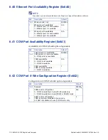
Page 72: ...rt 1 is not available 1 Ethernet port 1 is available N A 0 Ethernet port 0 availability 0 Ethernet port 0 is not available 1 Ethernet port 0 is available N A Bits Description Default 7 to 2 COM ports 8 to 3 availability COM ports 8 to 3 are not available 0 COM port is not available 000000b 1 COM2 availability 0 COM2 is not available 1 COM2 is available N A 0 COM1 availability COM1 is always availa...

Page 73: ...port is not available 0 Bits Description Default 7 to 3 SATA ports 7 to 3 availability SATA ports 7 to 3 are not available 0 SATA port is not available 00000b 2 SATA port 2 availability 0 SATA port 2 is not available 1 SATA port 2 is available N A 1 SATA port 1 availability 0 SATA port 1 is not available 1 SATA port 1 is available N A 0 SATA port 0 availability SATA port 0 is always available 1 SA...

Page 74: ...6 52 Display Port Display Availability Register 0x6AC As no Display Port displays are available this returns 0x00 Bits Description Default 7 to 2 Displays 7 to 2 are not available 000000b 1 Display 1 availability 0 Display 1 is not available 1 Display 1 is available N A 0 Display 0 availability Display 0 is always available 1 Display is available 1 Bits Description Default 7 to 1 Displays 7 to 1 V...

Page 75: ...t to port mapping is as follows 6 55 SSD Availability Register 0x6B1 Bits Description Default 7 Front panel I O availability Front panel I O is not available 0 Front panel I O not available 0 6 to 1 Reserved 000000b 0 Audio is not available 0b Bit Port 7 Ethernet 1 6 SATA 1 5 USB2 0 1 4 Video 1 3 Ethernet 0 2 SATA 0 1 USB2 0 0 0 Video 0 Bits Description Default 7 to 1 SSD7 to SSD1 availability SSD...

Page 76: ...SSD1 availability SSD7 to SSD1 are not supported 0 Hardware Secure Erase not available 0000000b 0 SSD0 availability 0 Hardware Secure Erase not available 1 Hardware Secure Erase available 1 Bits Read Write Description Default 7 to 3 Read only COM8 to COM4 UART enable COM8 to COM4 UARTs are not available 00000b 2 Read Write COM3 UART enable 1 COM3 UART is enabled 0 COM3 UART is disabled and will no...

Page 77: ...eiver in RS422 mode 0 COM2 transceiver in RS232 mode 0 0 Read Write COM1 mode 1 COM1 transceiver in RS422 mode 0 COM1 transceiver in RS232 mode 0 Bits Read Write Description Default 7 to 2 Read only COM8 to COM3 Auto Direction Control mode COM8 to COM3 are not available 000000b 1 Read Write COM2 RS485 Auto Direction Control mode 1 COM2 RS485 Auto Direction Control enabled 0 COM2 RS485 Auto Directi...

Page 78: ...SD7 to SSD1 hardware erase SSD7 to SSD1 are not supported 0 Hardware erase not available 0000000b 0 Read Write SSD0 hardware erase 0 Hardware Erase pin active 1 Hardware Erase pin negated 0 Bits Read Write Description Default 7 to 1 Read only SSD7 to SSD1 cache flush SSD7 to SSD1 are not supported 0 Cache flush not available 0000000b 0 Read Write SSD0 cache flush 0 Cache Flush pin active 1 Cache F...

Page 79: ...daisy chain status 1 Chain fault 0 Chain OK N A Bits Description Default 7 SYSCON status 1 SBC347A is fitted into a System Controller slot SYSCON backplane pin is low 0 SBC347A is not fitted into a system controller slot SYSCON backplane pin not pulled low N A 6 NVMRO status 1 Backplane NVMRO signal is asserted 0 Backplane NVMRO signal is negated N A 5 VPX GAP pin status 1 GAP pin is high 0 GAP pi...

Page 80: ...e protection is not active when link P4 is fitted and the NVMRO backplane signal is negated N A 4 Reserved 0 3 Boot SPI FLASH main write protection statusab 1 Hardware write protection is active 0 Hardware write protection is not active N A 2 Boot SPI FLASH recovery write protection statusab 1 Hardware write protection is active 0 Hardware write protection is not active N A 1 NVRAM write protectio...

Page 81: ...oard ROM 01 Active boot ROM is the Recovery onboard ROM b Determined by the Boot from TAC link on the TAC and the Recovery Boot Link P3 on the SBC347A N A 4 SPD locationc 1 SBC347A booted using SPD EEPROM s located on the TAC 0 Board booted using SPD EEPROM s located onboard c Determined by the state of the SPD link on the TAC N A 3 Ethernet configuration ROM locationd 0 Board booted using onboard...

Page 82: ...n the SBC347A Figure 7 1 Front Connector Positions and Numbering NOTE The SBC347A s guide pin receptacles are unkeyed by default but may be keyed to customer requirements Contact Abaco for more details Figure 7 2 Rear Connector Position and Numbering Table 7 1 Connector Functions Connector Function P0 to P2 VPX interface P5 on rear of PWB TAC connector ...

Page 83: ...ments Pin A B C D E F G 1 VS2 VS2 VS2 None N C N C N C 2 VS2 VS2 VS2 None N C N C N C 3 VS3 VS3 VS3 None VS3 VS3 VS3 4 NVMRO SYSRESET GND N C GND N C N C 5 SM1_DATA SM0_CLK GND P3V3_AUX GND GA4 GAP 6 GA0 GA1 GND N C GND GA2 GA3 7 JTAG_TRST JTAG_TMS GND JTAG_TDI JTAG_TDO GND JTAG_TCLK 8 GND N C N C GND REF_CLK_P REF_CLK_N GND Table 7 3 J0 Pin Assignments Fin A B C D E F G H I 1 VS2 VS2 VS2 VS2 None...

Page 84: ... GND 7 PEG_RXP2 PEG_RXN2 GND PEG_TXP2 PEG_TXN2 GND COM2_CTS 8 GND PEG_RXP3 PEG_RXN3 GND PEG_TXP3 PEG_TXN3 GND 9 SATA0_RXP SATA0_RXN GND SATA0_TXP SATA0_TXN GND COM1_TXD 10 GND USB_P0_P USB_P0_N GND USB_P1_P USB_P1_N GND 11 USB_P0_PWR USB_P1_PWR GND USB_P2_PWR USB_P3_PWR GND COM1_RXD 12 GND USB_P2_P USB_P2_N GND USB_P3_P USB_P3_N GND 13 ETH0_0P ETH0_0N GND ETH0_1P ETH0_1N GND COM2_TXD 14 GND ETH0_2...

Page 85: ...PEG_TXP2 PEG_TXN2 GND GND COM2_CTS 8 GND GND PEG_RXP3 PEG_RXN3 GND GND PEG_TXP3 PEG_TXN3 GND 9 SATA0_RXP SATA0_RXN GND GND SATA0_TXP SATA0_TXN GND GND COM1_TXD 10 GND GND USB_P0_P USB_P0_N GND GND USB_P1_P USB_P1_N GND 11 USB_P0_PW R USB_P1_PW R GND GND USB_P2_PW R USB_P3_PW R GND GND COM1_RXD 12 GND GND USB_P2_P USB_P2_N GND GND USB_P3_P USB_P3_N GND 13 ETH0_0P ETH0_0N GND GND ETH0_1P ETH0_1N GND...

Page 86: ...01_RXP0 DP01_RXN0 GND DP01_TXP0 DP01_TXN0 GND COM1_CTS 6 GND DP01_RXP1 DP01_RXN1 GND DP01_TXP1 DP01_TXN1 GND 7 DP01_RXP2 DP01_RXN2 GND DP01_TXP2 DP01_TXN2 GND VGA_DDC_SDA 8 GND DP01_RXP3 DP01_RXN3 GND DP01_TXP3 DP01_TXN3 GND 9 N C N C GND N C N C GND VGA_DDC_SCL 10 GND N C N C GND N C N C GND 11 N C N C GND N C N C GND N C 12 GND N C N C GND N C N C GND 13 SATA1_RXP SATA1_RXN GND SATA1_TXP SATA1_T...

Page 87: ...D GND COM1_CTS 6 GND GND DP01_RXP1 DP01_RXN1 GND GND DP01_TXP1 DP01_TXN1 GND 7 DP01_RXP2 DP01_RXN2 GND GND DP01_TXP2 DP01_TXN2 GND GND VGA_DDC_SDA 8 GND GND DP01_RXP3 DP01_RXN3 GND GND DP01_TXP3 DP01_TXN3 GND 9 N C N C GND N C N C N C GND GND VGA_DDC_SCL 10 GND GND N C N C GND GND N C N C GND 11 N C N C GND GND N C N C GND GND N C 12 GND GND N C N C GND GND N C N C GND 13 SATA1_RXP SATA1_RXN GND G...

Page 88: ...1 PEG_RXN1 GND PEG_TXP1 PEG_TXN1 GND 7 PEG_RXP2 PEG_RXN2 GND PEG_TXP2 PEG_TXN2 GND COM2_CTS 8 GND PEG_RXP3 PEG_RXN3 GND PEG_TXP3 PEG_TXN3 GND 9 SATA0_RXP SATA0_RXN GND SATA0_TXP SATA0_TXN GND COM1_TXD 10 GND USB_P0_P USB_P0_N GND USB_P1_P USB_P1_N GND 11 USB_P0_PWR USB_P1_PWR GND USB_P2_PWR USB_P3_PWR GND COM1_RXD 12 GND USB_P2_P USB_P2_N GND USB_P3_P USB_P3_N GND 13 ETH0_0P ETH0_0N GND ETH0_1P ET...

Page 89: ...G_TXN1 GND 7 PEG_RXP2 PEG_RXN2 GND GND PEG_TXP2 PEG_TXN2 GND GND COM2_CTS 8 GND GND PEG_RXP3 PEG_RXN3 GND GND PEG_TXP3 PEG_TXN3 GND 9 SATA0_RXP SATA0_RXN GND GND SATA0_TXP SATA0_TXN GND GND COM1_TXD 10 GND GND USB_P0_P USB_P0_N GND GND USB_P1_P USB_P1_N GND 11 USB_P0_PWR USB_P1_PWR GND GND USB_P2_PWR USB_P3_PWR GND GND COM1_RXD 12 GND GND USB_P2_P USB_P2_N GND GND USB_P3_P USB_P3_N GND 13 ETH0_0P ...

Page 90: ...TS 6 GND DP01_RXP1 DP01_RXN1 GND DP01_TXP1 DP01_TXN1 GND 7 DP01_RXP2 DP01_RXN2 GND DP01_TXP2 DP01_TXN2 GND VGA_DDC_SDA 8 GND DP01_RXP3 DP01_RXN3 GND DP01_TXP3 DP01_TXN3 GND 9 SATA2_RXP SATA2_RXN GND SATA2_TXP SATA2_TXN GND VGA_DDC_SCL 10 GND N C DVI0_DDC_SDA GND DVI0_DDC_SCL DVI0_HPD GND 11 DVI0_DATA0_P DVI0_DATA0_N GND DVI0_CLK_P DVI0_CLK_N GND N C 12 GND DVI0_DATA2_P DVI0_DATA2_N GND DVI0_DATA1_...

Page 91: ...XN1 GND GND DP01_TXP1 DP01_TXN1 GND 7 DP01_RXP2 DP01_RXN2 GND GND DP01_TXP2 DP01_TXN2 GND GND VGA_DDC_SDA 8 GND GND DP01_RXP3 DP01_RXN3 GND GND DP01_TXP3 DP01_TXN3 GND 9 SATA2_RXP SATA2_RXN GND SATA2_TXP SATA_TXN GND GND VGA_DDC_SCL 10 GND GND DVI0_DDC_SDA GND GND DVI0_DDC_SCL DVI0_HPD GND 11 DVI0_DATA0_P DVI0_DATA0_N GND GND DVI0_CLK_P DVI0_CLK_N GND GND N C 12 GND GND DVI0_DATA2_P DVI0_DATA2_N G...

Page 92: ... or RTM or driven low under software control by the SBC347A if configured as System Controller The FPGA Backplane Status Register 0x6CA shows the state JTAG_TCLK JTAG_TDO JTAG_TDI JTAG_TMS JTAG_TRST JTAG Test Clock Test Data Out Tx from SBC347A Test Data In Rx to SBC347A from test device Test Mode Select and Test Reset REF_CLK_P N OpenVPX Reference Clock differential signals Optionally used as 100...

Page 93: ...al RS422 mode Clear To Send input signal RS232 mode or Receive Data B signal RS422 mode See Section 5 8 1 RS422 RS485 Mode on page 42 PCIE_RST Reserved for future use not currently implemented BITFAIL Open drain BIT Fail drive for system level BIT Fail VGA_RED VGA_GREEN VGA_BLUE VGA_HSYNC VGA_VSYNC VGA_DDC_DATA VGA_DDC_CLK VGA Red Green Blue Horizontal Synchronization Vertical Synchronization Disp...

Page 94: ...0527837 000 Rev A 0 7 2 P5 Connector TAC This 80 way Molex connector where fitted is for Factory Field Application Engineer use only It provides an interface between the TAC and onboard programmable devices The pinout for the TAC connector is for Factory use only ...

Page 95: ...atible Able to generate edge or level triggered interrupts PCI Express Option x2 x4 PCH 1 x8 split between VPX P1 and P2 from CPU PCI GEN1 2 capable PCIe GEN1 2 3 capable Video 1 VGA 1 Optional DVI Thermal Sensors Board ambient CPU die PCIe Switch die temperatures All accessible via BMM Timers Three 82C54 equivalent internal to PCH Two 32 bit General purpose timers Programmable interrupt generatio...

Page 96: ... VPX Vs2 12V_AUX or 12V_AUX supplies A 2 2 Current Consumption When operating in Turbo mode up to 3 4 GHz and with the CPU cores working under absolute maximum load conditions the SBC347A will dissipate a maximum of 75W Current consumption values for SBC347A are shown below TIP The figures quoted above represent the requirements of the SBC347A under certain conditions When specifying system power ...

Page 97: ...COM1 serial port 1x external SATA Gen2 drive USB keyboard including a USB1 0 hub USB mouse Windows 7 idle Maximum Proprietary test software running under Windows 7 configured to exercise all main functional blocks simultaneously The CPU usage is 100 Turbo mode is off Peak Proprietary test software capable of exercising the CPU to maximum power conditions Turbo mode is on Table A 6 Current Consumpt...

Page 98: ... ANSI VITA51 1 2008 R2013 Specification This prediction relates only to the electronic components mechanical components are not included These failure rates are based only on the components and connectors fitted to the board at delivery Table A 9 Reliability MTBF Environment Temp Fail Rate fpmh MTBF Hours Ground Benign 30 C 2 738737 365 132 Ground Fixed 40 C 11 241661 88 955 Ground Mobile 45 C 26 ...

Page 99: ...10 Convection cooled Environmental Specifications Build Style Temperature C Vibration Shock Humidity Comments Standard Level 1 Operating 0 to 55 with airflow of 300 lfm Storage 50 to 100 Random 0 002 g2 Hz from 10 to 2000 Hz Sine 2 g from 5 to 500 Hz 20 g peak sawtooth 11 ms duration Up to 95 RH Commercial grade cooled by forced air for use in benign environments and software development applicati...

Page 100: ...equency this means that for a given build level a maximum CPU operating frequency is achievable For more details contact your nearest Abaco sales office or agent and see Appendix C Thermal Derating on page 95 Table A 12 Product Options SBC347A A B C D E F G H Ruggedization Level Processor and Frequency RAM NAND I O Firmware BMM Pitch 1 0 8 pitch VITA 46 mechanics 6 1 pitch VITA 48 mechanics 0 Rese...

Page 101: ...ation can be altered by the user using BIOS set up screens and these settings are stored in nonvolatile memory A 7 2 Built In Test BIT probes from the lowest level of discrete onboard hardware up to Line Replaceable Unit LRU level within a system ensuring the highest degree of confidence in system integrity BIT includes comprehensive configuration facilities allowing automatic initialization tests...

Page 102: ...h the SBC346ARTM depending on the development system being used NOTE The RTM contains PCIe redrivers that are limited to Gen2 When using the SBC347A with the SBC346ARTM the user must ensure that the PEG Port 0 is set to Gen1 or Gen2 in the BIOS setup TIP When using an Abaco SCVPX3U 12 starter chassis the SBC346RTM is required ...

Page 103: ... Table B 1 Volatile Memory Memory Type Size User Modifiable User Data Access Function Process to Clear DDR3 SDRAM 16 GBytes Yes Yes Contains run time data Power off On die processor shared cache 6 MBytes No No Improved memory performance Power off Chipset CMOS SRAM 256 bytes No Yes Real Time Clock data Power off including VBAT supply SRAM 35 Kbit No No Internal FPGA configuration Power off SRAM 15...

Page 104: ...us NVRAM FRAM 512 KByte devices Yes Yes Yes User defined parameters Can be cleared by any utility capable of writing to I O space Flash 2 MByte No No Yes Ethernet device configuration Can be cleared by any utility capable of writing to the LAN SPI bus FPGA N A No Yes N A Powerup reset logic glue logic LPC registers timers Watchdog NVRAM access JTAG via TAC EEPROM 40 Kbit No Yes No TPM key storage ...

Page 105: ...s are of the form SBC347A y1xxxxxx where y is the build level See Section A 6 ʺProduct Codesʺ on page 100 for details of the other options NOTE These values are preliminary based on the SBC347A and are subject to change without notice NOTE The thermal data for the above table was determined while the units were running multi threaded test software used to stress CPU memory and I O functions simult...

Page 106: ...ata Terminal Equipment ECC Error Checking and Correction EMI Electromagnetic Interference ETI Elapsed Time Indicator FPMH Failures Per Million Hours FRAM Ferro electric Random Access Memory FRU Field Replaceable Unit GA Geographic Addressing GbE Gigabit Ethernet GPIO General Purpose Input Output IPMI Intelligent Platform Management Interface ISA Industry Standard Architecture JEDEC Joint Electroni...

Page 107: ...Board RSA Rivest Shamir and Aldeman RTC Real Time Clock RTM Rear Transition Module RTS Ready to Send SBC Single Board Computer SKU Stock Keep Unit SLC Single Level Cell SMBus Serial Management Bus SPD Serial Presence Detect SPI Serial Peripheral Interconnect SSD Solid State Drive TAC Test Access Card SBC326TST TCG Trusted Computing Group TPM Trusted Platform Monitor UART Universal Asynchronous Rec...

Page 108: ...ite Enable 20 Descriptions 20 P3 20 P4 20 Positions 19 Recovery Boot 20 Configuration EEPROMs 20 48 Connecting to SBC346 23 Connectors 82 Backplane 83 J0 83 J1 89 J2 91 P0 83 P1 88 P2 90 P5 94 Positions and Numbering 82 Signal Descriptions 92 TAC 94 Convection cooled 99 Cooling 16 99 Core i7 processor 14 15 35 45 Current Consumption 96 D Data Plane Fabric 39 Dimensions 97 DIP Switch 48 Documentati...

Page 109: ... BMM BMC Control 63 Board ID 61 Board ID String 62 Board Jumper Link Status 80 Board Revision 61 Boot Location Status 81 COM Port 4 Wire Configuration 72 COM Port Availability 72 COM Port Enable 76 COM Port Loopback Enable 77 COM Port Mode 77 COM Port Modem Configuration 73 COM Port RS485 Auto Direction Control 77 Display Availability 74 Display Port Display Availability 74 DVI HDMI Display Availa...

Page 110: ...te Protection Status 80 Related Documents 4 Reliability 98 Resets 57 Board Reset LED 54 Maskable 38 Sequence and Timing 24 Returns 5 RTMs 23 102 S Safety Notices 16 SATA 43 Activity LED 55 SDRAM 36 Serial I O 41 Shock 99 Size 97 Sleep State LEDs 55 Software Support 101 Specifications 95 Electrical 96 Environmental 99 Mechanical 97 Technical 95 SSD 37 Activity LED 55 Storage Environment 99 T Techni...

Page 111: ...NTENTS ARE PROVIDED AS IS WITH NO REPRESENTATIONS OR WARRANTIES OF ANY KIND WHETHER EXPRESS OR IMPLIED INCLUDING BUT NOT LIMITED TO WARRANTIES OF DESIGN MERCHANTABILITY OR FITNESS FOR A PARTICULAR PURPOSE ALL OTHER LIABILITY ARISING FROM RELIANCE ON ANY INFORMATION CONTAINED HEREIN IS EXPRESSLY DISCLAIMED Abaco Systems Information Centers Americas 1 866 652 2226 866 OK ABACO or 1 256 880 0444 Inte...

Reviews: