FMC30RF User Manual
r1.3
UM015
- 10 -
5 Modes of operation
The FMC30RF support different modes of operation; TDD and FDD.
TRF372017
TRF3765
TRF371109
TRF371125
AFE7225
CDCE62005
FMC
LPC
REF OUT
REF IN
RX CLK
TX CLK
LO
REF
REF
RF I/O
RF IN
ATT
LNA_OUT
* not avalable from front panel
TX VCO IN
TX LO OUT
RX VCO IN
RX LO OUT
LNA_BYPASS_CTRL
TRX_SWITCH_CTRL
TX_VCO_CTRL
RX_VCO_CTRL
TCXO
30.72MHz
CDCE65005_REFEN
SEC_REF
PRI_REF
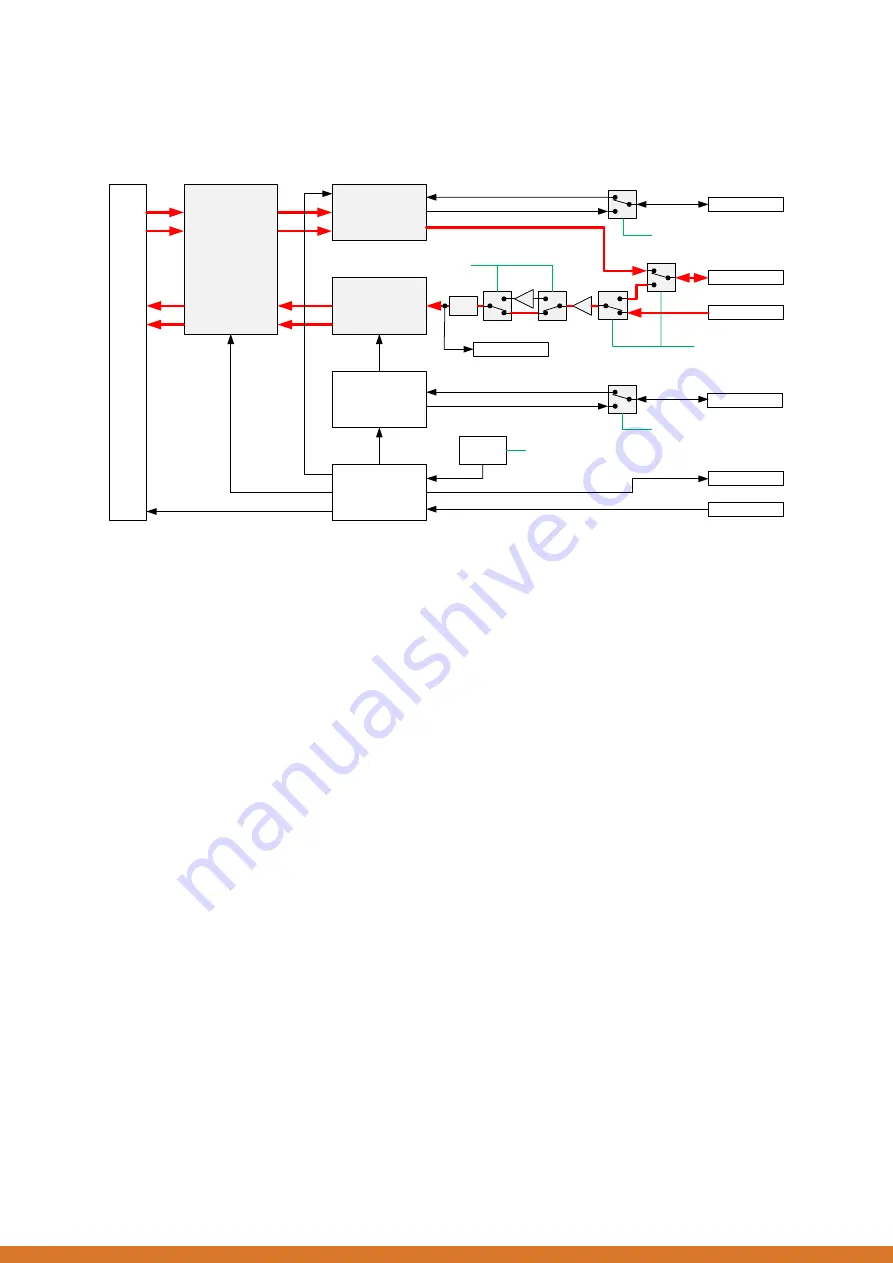
Figure 5: Signal Path
5.1 Time-Division Duplex (TDD)
The FMC30RF supports TDD using the RF I/O connector. The RF I/O connector is either
receiving (TRX_SWITCH_CTRL=0) or transmitting (TRX_SWITCH_CTRL=1). The
TRX_SWITCH_CTRL signal should be driven by the FPGA trough the FMC connector.
5.2
Frequency-Division Duplex (
FDD)
The FMC30RF supports FDD using the RF I/O connector for transmitting and the RF IN
connector for receiving. The TRX_SWITCH_CTRL signal should be driven high by the FPGA
trough the FMC connector.
5.3 Multiple-Input Multiple-Output (MIMO)
With two FMC30RF boards a 2x2 MIMO setup can be realised.

