FMC30RF User Manual
r1.3
UM015
- 11 -
TRF372017
TRF3765
TRF371109
TRF371125
AFE7225
FMC
LPC
REF OUT
REF IN
RX CLK
TX CLK
LO
REF
REF
RF I/O
RF IN
ATT
LNA_OUT
* not avalable f rom front panel
TX VCO IN
TX LO OUT
RX VCO IN
RX LO OUT
LNA_BYPASS_CTRL
TRX_SWITCH_CTRL
TX_VCO_CTRL
RX_VCO_CTRL
TCXO
30.72MHz
CDCE65005_REFEN
U0P/N
U4P
CDCE62005
U3P
U2P
U1P/N
CLK_M2C_P/N
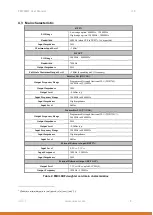
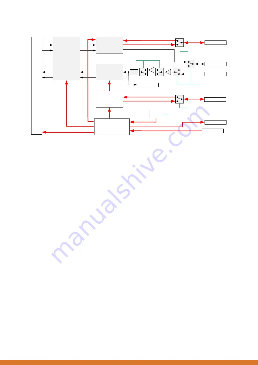
Figure 6: Clock paths
6 Controlling the FMC30RF
Good knowledge of the internal structure and communication protocol of relevant on-board
devices is required for controlling the FMC30RF. This document only provides guidelines for
programming the devices. For detailed information it is recommended to refer to the datasheets
listed in the related documents section of this document.
6.1 Guidelines for controlling the RF path
The following control signals controls the RF frontend;
•
TRX_SWITCH_CTRL
•
LNA_BYPASS_CTRL
•
RF_ATT_V[1..5]
Refer to Appendix A for a description of these signals.
The LNA in the RX path depends on the RF coverage specified at the time of order:
-
RF coverage option 1 (400MHz – 1200MHz):
SKY67101-396LF
-
RF coverage option 2 (1200MHz – 3000MHz):
SKY67100-396LF
The gain is 18-20dB for each LNA stage.
6.2 Guidelines for controlling the CDCE62005
The following control signals connect from the FMC connector to the CDCE62005;
•
SCLK (shared with other devices)
•
SDATA (shared with other devices)
•
CDCE62005_CS#
•
CDCE62005_SDOUT
•
CDCE62005_PD#
•
CDCE62005_SYNC#

