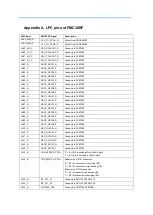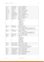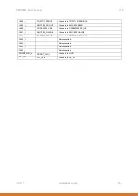
Appendix A LPC pin-out FMC30RF
FMC label
FMC30RF Signal
Description
CLK0_M2C_N
CLK_TO_FPGA_N
Output from CDCE62005
CLK0_M2C_P
CLK_TO_FPGA_P
Output from CDCE62005
LA00_N_CC
ADC_DCLKOUT_N
Connects to AFE7225
LA00_P_CC
ADC_DCLKOUT_P
Connects to AFE7225
LA01_N_CC
ADC_FCLKOUT_N
Connects to AFE7225
LA01_P_CC
ADC_FCLKOUT_P
Connects to AFE7225
LA02_N
ADCB_DATA1_N
Connects to AFE7225
LA02_P
ADCB_DATA1_P
Connects to AFE7225
LA03_N
ADCB_DATA0_N
Connects to AFE7225
LA03_P
ADCB_DATA0_P
Connects to AFE7225
LA04_N
ADCA_DATA1_N
Connects to AFE7225
LA04_P
ADCA_DATA1_P
Connects to AFE7225
LA05_N
ADCA_DATA0_N
Connects to AFE7225
LA05_P
ADCA_DATA0_P
Connects to AFE7225
LA06_N
DAC_FCLKIN_N
Connects to AFE7225
LA06_P
DAC_FCLKIN_P
Connects to AFE7225
LA07_N
DACA_DATA1_N
Connects to AFE7225
LA07_P
DACA_DATA1_P
Connects to AFE7225
LA08_N
DACA_DATA0_N
Connects to AFE7225
LA08_P
DACA_DATA0_P
Connects to AFE7225
LA09_N
DACB_DATA0_N
Connects to AFE7225
LA09_P
DACB_DATA0_P
Connects to AFE7225
LA10_N
DAC_DCLKIN_N
Connects to AFE7225
LA10_P
DAC_DCLKIN_P
Connects to AFE7225
LA11_N
DAC_SYNCIN_N
Connects to AFE7225
LA11_P
DAC_SYNCIN_P
Connects to AFE7225
LA12_N
DACB_DATA1_N
Connects to AFE7225
LA12_P
DACB_DATA1_P
Connects to AFE7225
LA13_N
LNA_BYPASS_CTRL
‘0’ = 2
nd
LNA is excluded from the RX path
‘1’ = 2
nd
LNA is included in the RX path
LA13_P
TRX_SWITCH_CTRL
Behavior on RF I/O connector;
‘0’ = RF I/O connector is receiving (RX)
‘1’ = RF I/O connector is transmitting (TX)
Behavior on RF IN connector;
‘0’ = RF IN connector is disconnected
‘1’ = RF IN connector is receiving (RX)
LA14_N
RF_ATT_V1
Connects to SKY12329-350LF V1
LA14_P
RF_ATT_V2
Connects to SKY12329-350LF V2
LA15_N
TRF3765_CS#
Connects to TRF3765 STROBE


