background image

FMC30RF User Manual 


r1.3 


UM015


            www.abaco.com 


- 18 - 

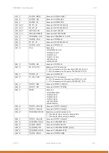
LA15_P 

AFE7225_RESET 

Connects to AFE7225 RESET 

LA16_N 

AFE7225_CS# 

Connects to AFE7225 SEN 

LA16_P 

AFE7225_PD 

Connects to AFE7225 PDN 

LA17_N_CC 

RF_ATT_V4 

Connects to SKY12329-350LF V4 

LA17_P_CC 

RF_ATT_V3 

Connects to SKY12329-350LF V3 

LA18_N_CC 

AMC7823_CS# 

Connects to AMC7823 SS 

LA18_P_CC 

AMC7823_RESET# 

Connects to AMC7823 RESET 

LA19_N 

CDCE62005_LOCK 

Connects to CDCE62005 PLL_LOCK 

LA19_P 

TRF3765_LOCK 

Connects to TRF3765 LD 

LA20_N 

RF_ATT_V5 

Connects to SKY12329-350LF V5 

LA20_P 

TRF3720_LOCK 

Connects to TRF3720 LD 

LA21_N 

SCLK 

Connects to: 

- CDCE62005 SPI_CLK 

- TRF3765 CLOCK 

- TRF3720 CLK 

- TRF3711 CLOCK 

- AFE7225 SCLK 

- AMC7823 SCLK 

LA21_P 

TRF3720_CS# 

Connects to TRF3720 LE 

LA22_N 

RX_VCO_CTRL 

Behavior on RX CLK connector; 

‘0’ = RX CLK connector is VCO output from TRF3765 LO4_OUT 

‘1’ = RX CLK connector is VCO input to TRF3765 EXTVCO_IN 

LA22_P 

TRF3720_PS 

Connects to TRF3720 PS 

LA23_N 

TX_VCO_CTRL 

Behavior on TX CLK connector; 

‘0’ = TX CLK connector is VCO output from TRF3720 LO_OUT 

‘1’ = TX CLK connector is VCO input to TRF3720 EXT_VCO 

LA23_P 

TRF3711_PD# 

Connects to TRF3711 CHIP_EN 

LA24_N 

TRF3711_CS# 

Connects to TRF3711 STROBE 

LA24_P 

SDATA 

Connects to 

- CDCE62005 MOSI 

- TRF3765 DATA 

- TRF3720 DATA 

- TRF3711 DATA 

- AFE7225 SDATA 

- AMC7823 MOSI 

LA25_N 

TRF3711_GAIN_B0 

Connects to TRF3711 GAIN_B0 

LA25_P 

TRF3711_GAIN_B1 

Connects to TRF3711 GAIN_B1 

LA26_N 

CDCE62005_REFEN 

Behavior on on-board reference clock; 

‘0’ = the on-board reference clock is powered down 

‘1’ = the on-board reference clock is enabled 

LA26_P 

TRF3711_GAIN_B2 

Connects to TRF3711 GAIN_B2 

LA27_N 

CDCE62005_SDOUT 

Connects to CDCE62005 MISO 

LA27_P 

AFE7225_SDOUT 

Connects to AFE7225 SDOUT 

LA28_N 

CDCE62005_PD# 

Connects to CDCE62005 POWER_DOWN 

LA28_P 

CDCE62005_SYNC# 

Connects to CDCE62005 SYNC 

LA29_N 

TRF3720_SDOUT 

Connects to TRF3720 RDBK 

Summary of Contents for FMC30RF

Page 1: ... abaco com 1 FMC30RF User Manual Abaco Systems USA Support Portal This document is the property of Abaco Systems and may not be copied nor communicated to a third party without the written permission of Abaco Systems Abaco Systems 2015 ...

Page 2: ...05 30 Draft 0 1 2012 05 30 Release after review 1 0 2012 10 05 Additional info on LNA and reference oscillator 1 1 2014 06 11 Update voltage monitoring section Additional info in Figure 5 and pin out 1 2 2015 02 12 Added RF input analog line up description updated RF in out characteristics 1 3 ...

Page 3: ...n Duplex TDD 10 5 2 Frequency Division Duplex FDD 10 5 3 Multiple Input Multiple Output MIMO 10 6 Controlling the FMC30RF 11 6 1 Guidelines for controlling the RF path 11 6 2 Guidelines for controlling the CDCE62005 11 6 3 Guidelines for controlling the TRF3765 12 6 4 Guidelines for controlling the TRF3711 12 6 5 Guidelines for controlling the TRF3720 12 6 6 Guidelines for controlling the AFE7225 ...

Page 4: ...Low Voltage Transistor Logic level LSB Least Significant Bit s LVDS Low Voltage Differential Signaling MGT Multi Gigabit Transceiver MSB Most Significant Bit s PCB Printed Circuit Board PLL Phase Locked Loop PSSR Power Supply Rejection Ratio Table 1 Glossary 1 2 Related Documents FPGA Mezzanine Card FMC standard ANSI VITA 57 1 2010 CDCE62005 datasheet TI August 2011 TRF3765 datasheet TI November 2...

Page 5: ...ial communication busses Furthermore the card is equipped with power supply and temperature monitoring and offers several power down modes to switch off unused functions TRF372017 TRF3765 TRF371109 TRF371125 AFE7225 CDCE62005 FMC LPC REF OUT REF IN RX CLK TX CLK LO REF REF RF I O RF IN ATT LNA_OUT TCXO 30 72MHz not avalable from front panel TX VCO IN TX LO OUT RX VCO IN RX LO OUT LNA_BYPASS_CTRL T...

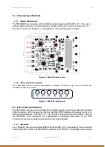
Page 6: ...connector type Six connectors are available on the front panel TX CLK RF I O RF IN RX CLK REF OUT REF IN Figure 3 FMC30RF bezel layout 4 2 Electrical specifications The FMC30RF card uses a mix of LVDS and LVCMOS signals According to the FMC standard VADJ should be 2 5V to support LVDS but the FMC30RF is designed to accept any level on VADJ ranging between 1 65V and 5 5V VIO_B_M2C connections are c...

Page 7: ...CC and LA01_CC respectively The ADC data pairs are mapped to LA02 to LA05 The DAC clock frame and data pairs are mapped to LA06 to LA12 Since all pairs are outputs as seen from the FPGA there is no need to have the clock and frame pair on clock capable pins LA13 to LA31 are used for low speed single ended communication and control signals The remaining connections LA32 LA33 are used left unconnect...

Page 8: ...dBm and can be applied to the board when the total gain of the analog line up is set to minimum This is done by Bypass LNA2 Set the stepped attenuator to 32dB attenuation Set the BB gain of the TRF3711 to 0dB default setting is 15dB refer to the datasheet of the TRF3711 Applying a signal of 3dBm to the first stage LNA drives the LNA close to its input 1dB compression point ...

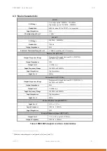
Page 9: ...Impedance 50Ω Output Level 0 5dBm typ Input Frequency Range 300MHz to 4800MHz Input Impedance High impedance Input Level 0dBm Transmitter LO TX CLK Output Frequency Range Programmable trough fractional PLL TRF372017 300MHz to 4800MHz Output Impedance 50Ω Output Level 0 5dBm typ Input Frequency Range 300MHz to 4800MHz Input Impedance High impedance Input Level 0dBm External Reference Input REF IN I...

Page 10: ... SEC_REF PRI_REF Figure 5 Signal Path 5 1 Time Division Duplex TDD The FMC30RF supports TDD using the RF I O connector The RF I O connector is either receiving TRX_SWITCH_CTRL 0 or transmitting TRX_SWITCH_CTRL 1 The TRX_SWITCH_CTRL signal should be driven by the FPGA trough the FMC connector 5 2 Frequency Division Duplex FDD The FMC30RF supports FDD using the RF I O connector for transmitting and ...

Page 11: ...programming the devices For detailed information it is recommended to refer to the datasheets listed in the related documents section of this document 6 1 Guidelines for controlling the RF path The following control signals controls the RF frontend TRX_SWITCH_CTRL LNA_BYPASS_CTRL RF_ATT_V 1 5 Refer to Appendix A for a description of these signals The LNA in the RX path depends on the RF coverage s...

Page 12: ...he FMC connector to the TRF3711 SCLK shared with other devices SDATA shared with other devices TRF3711_CS TRF3711_SDOUT TRF3711_PD TRF3711_GAIN_B 0 2 Refer to Appendix A for a description of these signals 6 5 Guidelines for controlling the TRF3720 The following control signals connect from the FMC connector to the TRF3720 SCLK shared with other devices SDATA shared with other devices TRF3720_CS TR...

Page 13: ... Max Amps Max Watt 3 3V 4 3 A 10 W 12V 2 1 A 12 W VADJ 2 5V 4 4 A 10 W VIO_B 2 5V 2 1 15 A 2 3 W Table 3 FMC standard power specification The power provided by the carrier card can be very noisy Special care is taken with the power supply generation on the FMC30RF card to minimize the effect of power supply noise on clock generation de modulation and data conversion Clean supply is derived from 3 ...

Page 14: ...5V0A_DAC TPS7A8001 132mA 3 8V à 3 3V 3V3A_DAC TPS7A8001 580mA 3 8V à 3 3V CDCE_3p3 TPS7A8001 201mA 5 5V à 4 0V RF_4p0 TPS7A8001 360mA 5 5V à 5 0V TRF3711_5p0 TPS74401 148mA 5 5V à 5 0V TRF3720_5p0 TPS74401 250mA 3 8V à 3 3V TRF3720_3p3 TPS74401 190mA 3 8V à 3 3V TRF3765_3p3 TPS63020 0 75A 3 3V à 5 5V TPS5430 1 30A 12V à 3 8V TPS7A8001 30mA 3 8V à 3 3V TCXO_3p3 1 4A 3 3V 0 5A 12V Typical power cons...

Page 15: ...vection cooling The air flow provided by the chassis fans the FMC30RF is enclosed in will dissipate the heat generated by the on board components A minimum airflow of 300 LFM is recommended For stand alone operations such as on a Xilinx development kit it is highly recommended to blow air across the FMC and ensure that the temperature of the devices is within the allowed range Abaco s warranty doe...

Page 16: ...side the host system which may be introduced through the system 11 Ordering information Part Number FMC30RF 2 1 1 1 Temperature Range Industrial 40o C to 85o C 1 Commercial 0o C to 70o C 2 Connector Type Standard Feature MMCX snap coupling 1 SSMC screw coupling 2 RF coverage 400MHz 1200MHz 1 1200MHz 3000MHz 2 Mil I 46058c Conformal Coating No Conformal Coating 1 Add Conformal Coating 2 Card Type F...

Page 17: ... LA07_N DACA_DATA1_N Connects to AFE7225 LA07_P DACA_DATA1_P Connects to AFE7225 LA08_N DACA_DATA0_N Connects to AFE7225 LA08_P DACA_DATA0_P Connects to AFE7225 LA09_N DACB_DATA0_N Connects to AFE7225 LA09_P DACB_DATA0_P Connects to AFE7225 LA10_N DAC_DCLKIN_N Connects to AFE7225 LA10_P DAC_DCLKIN_P Connects to AFE7225 LA11_N DAC_SYNCIN_N Connects to AFE7225 LA11_P DAC_SYNCIN_P Connects to AFE7225...

Page 18: ...65 LO4_OUT 1 RX CLK connector is VCO input to TRF3765 EXTVCO_IN LA22_P TRF3720_PS Connects to TRF3720 PS LA23_N TX_VCO_CTRL Behavior on TX CLK connector 0 TX CLK connector is VCO output from TRF3720 LO_OUT 1 TX CLK connector is VCO input to TRF3720 EXT_VCO LA23_P TRF3711_PD Connects to TRF3711 CHIP_EN LA24_N TRF3711_CS Connects to TRF3711 STROBE LA24_P SDATA Connects to CDCE62005 MOSI TRF3765 DATA...

Page 19: ...nnects to AMC7823 MISO LA30_P CDCE62005_CS Connects to CDCE62005 SPI_LE LA31_N AMC7823_GALR Connects to AMC7823 GALR LA31_P TRF3765_SDOUT Connects to TRF3765 READBACK LA32_N Not connected LA32_P Not connected LA33_N Not connected LA33_P Not connected PRSNT_M2C_L PRSNT_M2C_L Connects to GND PG_C2M PG_C2M Connects to PS_EN ...

Reviews: