FMC30RF User Manual
r1.3
UM015
- 7 -
0.01µA when SCL and SDA are kept at 3P3VAUX level. These signals may also be left floating
since pull-up resistors are present on the card.
4.2.2 JTAG
The FMC30RF card TDO pin is connected to the TDI pin (through an SN74LVC1G126 buffer)
to ensure continuity of the JTAG chain. TCK, TMS and TRST are left unconnected on the
FMC30RF.
4.2.3 FMC connector
The low-pin count connector has only bank LA available and two dedicated LVDS clock pairs.
The recommendations from AV57.1-2010 Table 14 have been taking into account resulting in
the following arrangement:
•
The ADC data clock pair (ADC_DCLKOUT) and ADC frame clock pair
(ADC_FCLKOUT) are connected to clock capable pins LA00_CC and LA01_CC
respectively. The ADC data pairs are mapped to LA02 to LA05.
•
The DAC clock, frame and data pairs are mapped to LA06 to LA12. Since all pairs are
outputs as seen from the FPGA, there is no need to have the clock and frame pair on
clock capable pins.
•
LA13 to LA31 are used for low speed single ended communication and control signals.
•
The remaining connections (LA32-LA33) are used left unconnected.
•
An LVDS output of the CDCE62005 is connected to a dedicated LVDS connections on
the FMC (CLK0_M2C). The other dedicated LVDS connection is not used.
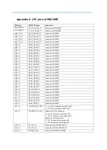
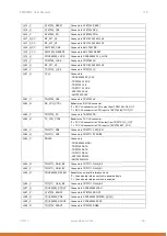
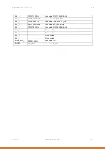
Refer also to the appendix for the detailed LPC connector pinout.
4.2.4 RF input
The RF input circuit comprises tuneable and fixed gain stages. The analog line-up is depicted
in Figure 4.
TRF371109
TRF371125
AFE7225
RF I/O
RF IN
ATT
LNA_BYPASS_CTRL
LNA1
+18dB
LNA2
+18dB
SW2
-0.5dB
SW1
-0.5dB
SW3
-0.5dB
ATT:
-1dB to
-32dB
BB Gain:
0dB to
+24dB
Figure 4: RF input analog line-up


