Parameters and firmware blocks
54
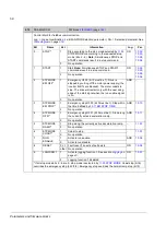
Note:
Pointing to a nonexisting bit will be interpreted as 0 (FALSE).
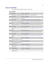
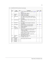
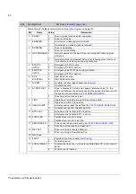
For additional parameter data, e.g. update cycles and fieldbus equivalents, see
chapter
.
Firmware blocks
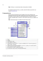
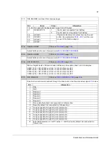
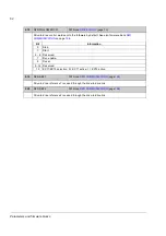
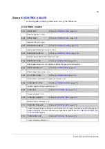
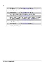
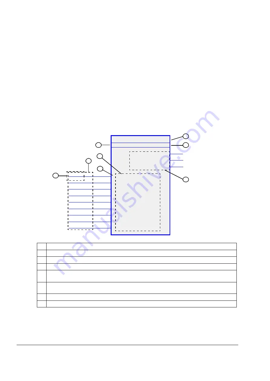
Firmware blocks accessible from the DriveSPC PC tool are described in the
parameter group most of the block inputs/outputs are included in. Whenever a block
has inputs or outputs outside the current parameter group, a reference is given.
Likewise, parameters have a reference to the firmware block they are included in (if
any).
Note:
Not all parameters are available through firmware blocks.
!
"#$$%&'
(
"#$$%&'
!( !
"#$$%&'
) (
"#$$%&'
* (
"#$$%&'
+
(
,
1
Inputs
2
Outputs
3
Input parameter values
4
Pointer parameter indicator “<“
5
Parameter 26.01 is set to value P.1.1, i.e. signal 1.01 SPEED ACT. The “7” means the signal can be
found on page 7 of DriveSPC.
6
ID of the time level (TL4) and time level (250 µs). Time level, i.e. update cycle, is application-specific.
See the time level of the block in DriveSPC.
7
Firmware block ID number in the application program
8
Firmware block execution order for the selected update cycle ID
2
3
6
7
8
4
5
1
Summary of Contents for ACSM1 Series
Page 1: ...ACSM1 Firmware Manual ACSM1 Speed and Torque Control Program...
Page 2: ......
Page 4: ......
Page 12: ...Table of contents 12...
Page 49: ...Drive control and features 49...
Page 282: ...Standard function blocks 282...
Page 306: ...Application program template 306...
Page 312: ...Control chain block diagrams 312...
Page 331: ...331...
Page 332: ...332...
Page 333: ......

