


Introducing the BIOS
User’s Manual
4-17
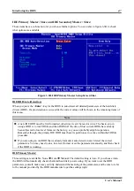
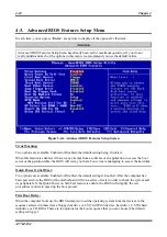
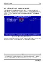
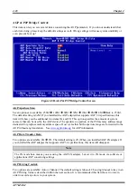
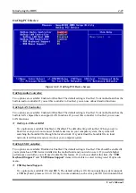
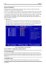
DIMM1&2 CMD Drive:
This item allows you to adjust the memory data drive strength. You can key in the HEX number into this
section. The minimum number is 0000, and maximum number is 00FF. Adjust the drive strength for
command sent to DDR SDRAM (This adjustment for DIMM 1 and DIMM 2 only). This will depend on
your DDR SDRAM specification and numbers to set. More DDR SDRAM DIMM installed, you may set
it to higher values.
DIMM3&4 CMD Drive:
This item allows you to adjust the memory data drive strength. You can key in the HEX number into this
section. The minimum number is 0000, and maximum number is 00FF. Adjust the drive strength for
command sent to DDR SDRAM (This adjustment for DIMM 3 and DIMM 4 only). This will depend on
your DDR SDRAM specification and numbers to set. More DDR SDRAM DIMM installed, you may set
it to higher values.
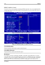
DRAM Access:
Two options are available: 2T
3T. The default setting is
3T
. This item allow you to choose the DRAM
access time cycle, 2T can let you get quick DRAM acess time than 3T, and 3Tis a general DRAM setting.
Enhance DRAM Performance:
Two options are available: Disabled or Enabled. The default setting is
Disabled
. This item can improve
your system DRAM performance.
DRAM Command Rate:
Two options are available: 2T Command or 1T Command. The default setting is
2T Command
. When the
host (northbridge) locates the desired memory address, it then processes the wait state of commands. Set
it to
2T Command
for system compatibility or to
1T Command
for system performance.
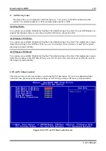
Write Recovery time
Two options are available: 2T or 3T. The default setting is
3T
. This is the period between two write times.
DRAM tWTR:
Two options are available: 1T or 3T. The default setting is
3T
. This is the Internal WRITE to READ
command delay time period.
DCLK Output Delay:
Eight options are available: 0 ps
150 ps
300 ps
450 ps
600 ps
750 ps
900 ps
1050
ps. The default setting is
0 ps
. The northbridge will send an output signal to clock buffer of DRAM
module, then clock buffer will feedback a signal to northbridge. The value you set will effect the delay
time for DCLK output signal. This item will effect the DRAM module’s stability, we suggestion you set
to
0 ps
.
Summary of Contents for AB-AT7-MAX2
Page 2: ......
Page 34: ...Chapter 2 AT7 MAX2 2 6 ...
Page 54: ...Chapter 3 AT7 MAX2 3 20 ...
Page 94: ...Chapter 5 AT7 MAX2 5 6 ...
Page 98: ...Chapter 6 AT7 MAX2 6 4 ...
Page 102: ...7 4 Chapter 7 AT7 MAX2 ...
Page 106: ...A 4 Appendix A AT7 MAX2 ...
Page 110: ...Appendix B AT7 MAX2 B 4 ...
Page 118: ...Appendix D AT7 MAX2 D 4 ...
Page 122: ...Appendix E AT7 MAX2 E 4 ...
Page 136: ...H 4 Appendix H AT7 MAX2 ...


