177
/
246
ABOV Semiconductor
I
2
C
Data Transfer
11.4.3
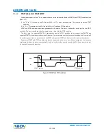
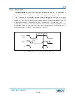
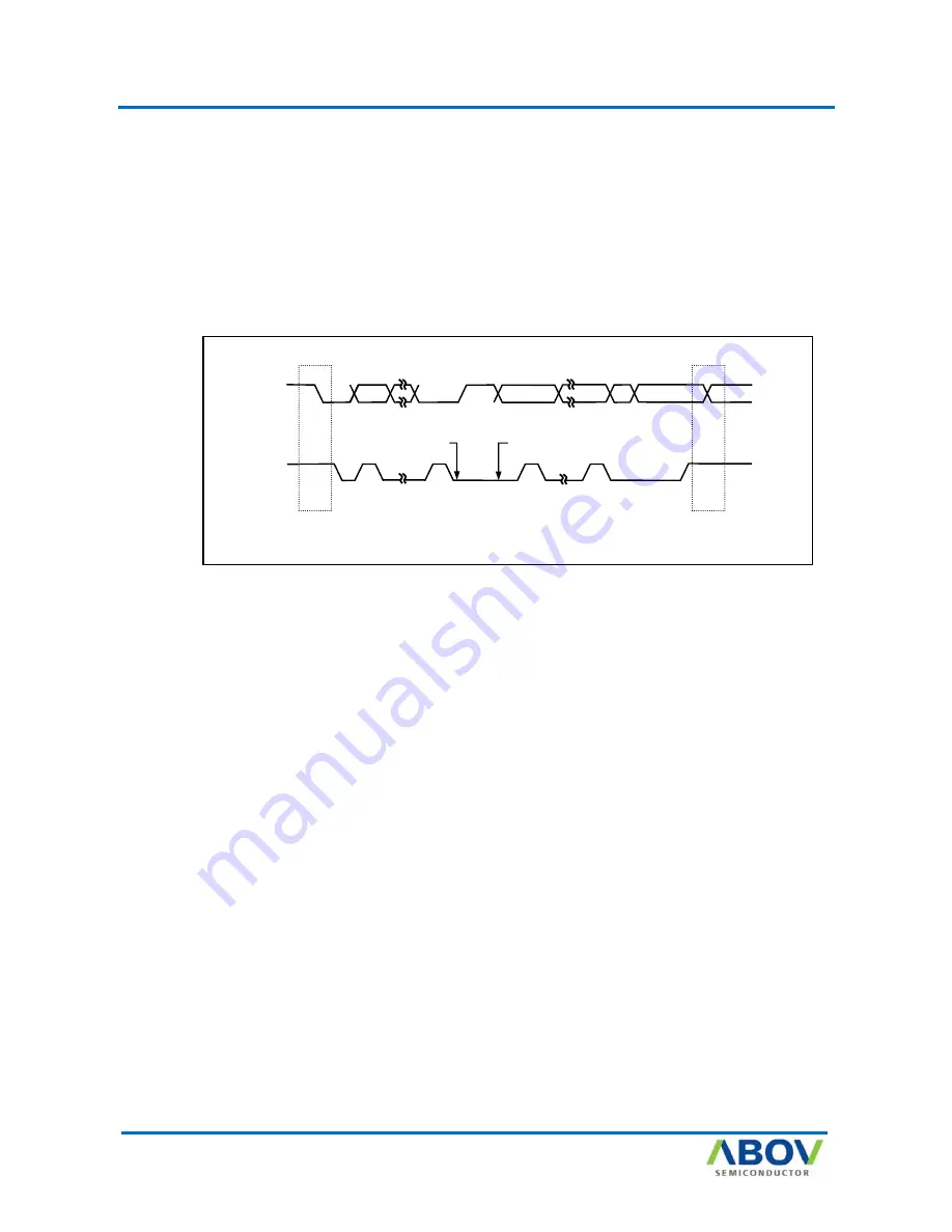
Every byte put on the SDA line must be 8-bits long. The number of bytes that can be transmitted per transfer is
unrestricted. Each byte has to be followed by an acknowledge bit. Data is transferred with the most significant bit (MSB)
first (see Figure 11.8). If a slave can’t receive or transmit another complete byte of data until it has performed some other
function, for example servicing an internal interrupt, it can hold the clock line SCL “L” to force the master into a wait state.
Data transfer then continues when the slave is ready for another byte of data and releases clock line SCL.
A message which starts with such an address can be terminated by generation of a STOP conditions, even during the
transmission of a byte. In this case, no acknowledge is generated.
Figure 11.8 I
2
C Bus data transfer
START or Repeated
START Condition
S
or
Sr
STOP or Repeated
START Condition
Sr
or
P
MSB
Acknowledgement
Signal from Slave
Acknowledgement
Signal from Slave
Byte Complete,
Interrupt within Device
Clock line held low
while interrupts are served.
1
9
1
9
ACK
ACK
SDA
SCL
Sr
P
Summary of Contents for AC30M1x32
Page 3: ...3 246 ABOV Semiconductor INTRODUCTION SECTION 1 INTRODUCTION ...
Page 4: ...4 246 4 246 AC30M1x64 1x32 ABOV Semiconductor OVERVIEW CHAPTER 1 ...
Page 18: ...18 246 18 246 ABOV Semiconductor AC30M1x64 1x32 CPU CHAPTER 2 ...
Page 22: ...22 246 22 246 ABOV Semiconductor AC30M1x64 1x32 Boot Mode CHAPTER 3 ...
Page 26: ...26 246 26 246 ABOV Semiconductor AC30M1x64 1x32 SECTION 2 PERIPHERALS ...
Page 27: ...27 246 ABOV Semiconductor System Control Unit SCU SYSTEM CONTROL UNIT SCU CHAPTER 1 ...
Page 69: ...69 246 ABOV Semiconductor Port Control Unit PCU PORT CONTROL UNIT PCU CHAPTER 2 ...
Page 85: ...85 246 ABOV Semiconductor General Purpose I O GPIO GENERAL PURPOSE I O GPIO CHAPTER 3 ...
Page 92: ...92 246 92 246 AC30M1x64 1x32 ABOV Semiconductor FLASH MEMORY CONTROLLER CHAPTER 4 ...
Page 105: ...105 246 ABOV Semiconductor Internal SRAM INTERNAL SRAM CHAPTER 5 ...
Page 107: ...107 246 ABOV Semiconductor Watch Dog Timer WATCH DOG TIMER WDT CHAPTER 6 ...
Page 113: ...113 246 ABOV Semiconductor 16 bit Timer 16 BIT TIMER CHAPTER 7 ...
Page 129: ...129 246 ABOV Semiconductor FRT FREE RUN TIMER FRT CHAPTER 8 ...
Page 134: ...134 246 134 246 ABOV Semiconductor AC30M1x64 1x32 FUNCTION DESCRIPTION 8 3 ...
Page 135: ...135 246 UART ABOV Semiconductor UNIVERSAL ASYNCHRONOUS CHAPTER 9 RECEIVER TRANSMITTER UART ...
Page 151: ...151 246 ABOV Semiconductor UART Figure 9 6 Transmit interrupt timing diagram ...
Page 152: ...152 246 152 246 ABOV Semiconductor AC30M1x64 1x32 SERIAL PERIPHERAL INTERFACE SPI CHAPTER 10 ...
Page 164: ...164 246 164 246 ABOV Semiconductor AC30M1x64 1x32 I2 C Interface CHAPTER 11 ...
Page 185: ...185 246 ABOV Semiconductor Motor PWM MOTOR PULSE WIDTH MODULATOR CHAPTER 12 MPWM ...
Page 215: ...215 246 ABOV Semiconductor Divider DIVIDER DIV64 CHAPTER 13 ...
Page 221: ...221 246 ABOV Semiconductor 12 BIT A D Converter 12BIT A D CONVERTER CHAPTER 14 ...
Page 235: ...235 246 ABOV Semiconductor CHARACTERISTIC SECTION 3 CHARACTERISTIC ...
Page 236: ...236 246 236 246 ABOV Semiconductor AC30M1x64 1x32 Electrical Characteristic CHAPTER 1 ...
Page 243: ...243 246 ABOV Semiconductor Package Package CHAPTER 2 ...

