103
/
246
ABOV Semiconductor
Flash Memory Controller
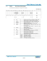
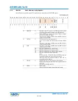
FM.RPROT
Flash Memory Read Protection Register
4.2.12
Internal flash memory read protection register. This registers will be update from OTP area of Flash while boot sequence,
so user cannot write or clear any bit directly.
FM.RPROT=0x4000_017C
31 30 29 28 27 26 25 24 23 22 21 20 19 18 17 16 15 14 13 12 11 10 9
8
7
6
5
4
3
2
1
0
LO
C
K
2
LO
C
K
1
JT
A
GD
IS
-
-
READ PROTECTIN
0
0
0
-
-
0xFF
RO
RO
RO
-
RW
31
LOCK2
Read protection level 2 state flag
30
LOCK1
Read protection level 1 state flag
29
JTAGDIS
JTAG disable state flag
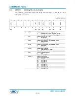
7
0
Unlock
By default, read protection disable (FM.RPROT = 0xFF)
LOCK1
Read protection level 1
Code protection mode enable, debug can be connected
Write 0x39 to activate LOCK1 (only can be written in Unlock
state)
Code in SRAM or debugger cannot read flash area
When flash was read from SRAM or debugger, 0xA5A5A5A5 will
be return as read data
LOCK2
Read protection level 2
Code protection mode enable, debug cannot be connected
Write any value except 0x39(include 0xFF) to activate LOCK2
(only can be written in Unlock state or LOCK1)
When flash was read from SRAM, 0xA5A5A5A5 will be return as
read data
Flash Erase and Program examples
4.2.13
The basic step of Flash memory program consists with following three steps. Minimum Program or Erase unit is a Page
and 32-word (128-byte) become a page.
(1)
Pre-program of target Page before erase operation
(2)
Page Erase
(3)
Page Program
For every erase operations, pre-program operation is needed to prevent over erase of flash memory cells.
User must enable 40MHz internal oscillator first to erase or program flash.
(1)
Pre-program and Erase example
A.
Flash mode enable to write FM.CR register (write 0x5A and then write 0xA5 into FMMR)
B.
Set FM.TMR register to be 0.5ms operation (based on 40MHz Int OSC clock)
C.
Set target Page address in FM.AR
D.
Set PMODE bit first
E.
set PPGM, WE, PGM bits of FMCR
Summary of Contents for AC30M1x64
Page 3: ...3 246 ABOV Semiconductor INTRODUCTION SECTION 1 INTRODUCTION...
Page 4: ...4 246 4 246 AC30M1x64 1x32 ABOV Semiconductor OVERVIEW CHAPTER 1...
Page 18: ...18 246 18 246 ABOV Semiconductor AC30M1x64 1x32 CPU CHAPTER 2...
Page 22: ...22 246 22 246 ABOV Semiconductor AC30M1x64 1x32 Boot Mode CHAPTER 3...
Page 26: ...26 246 26 246 ABOV Semiconductor AC30M1x64 1x32 SECTION 2 PERIPHERALS...
Page 27: ...27 246 ABOV Semiconductor System Control Unit SCU SYSTEM CONTROL UNIT SCU CHAPTER 1...
Page 69: ...69 246 ABOV Semiconductor Port Control Unit PCU PORT CONTROL UNIT PCU CHAPTER 2...
Page 85: ...85 246 ABOV Semiconductor General Purpose I O GPIO GENERAL PURPOSE I O GPIO CHAPTER 3...
Page 92: ...92 246 92 246 AC30M1x64 1x32 ABOV Semiconductor FLASH MEMORY CONTROLLER CHAPTER 4...
Page 105: ...105 246 ABOV Semiconductor Internal SRAM INTERNAL SRAM CHAPTER 5...
Page 107: ...107 246 ABOV Semiconductor Watch Dog Timer WATCH DOG TIMER WDT CHAPTER 6...
Page 113: ...113 246 ABOV Semiconductor 16 bit Timer 16 BIT TIMER CHAPTER 7...
Page 129: ...129 246 ABOV Semiconductor FRT FREE RUN TIMER FRT CHAPTER 8...
Page 134: ...134 246 134 246 ABOV Semiconductor AC30M1x64 1x32 FUNCTION DESCRIPTION 8 3...
Page 135: ...135 246 UART ABOV Semiconductor UNIVERSAL ASYNCHRONOUS CHAPTER 9 RECEIVER TRANSMITTER UART...
Page 151: ...151 246 ABOV Semiconductor UART Figure 9 6 Transmit interrupt timing diagram...
Page 152: ...152 246 152 246 ABOV Semiconductor AC30M1x64 1x32 SERIAL PERIPHERAL INTERFACE SPI CHAPTER 10...
Page 164: ...164 246 164 246 ABOV Semiconductor AC30M1x64 1x32 I2 C Interface CHAPTER 11...
Page 185: ...185 246 ABOV Semiconductor Motor PWM MOTOR PULSE WIDTH MODULATOR CHAPTER 12 MPWM...
Page 215: ...215 246 ABOV Semiconductor Divider DIVIDER DIV64 CHAPTER 13...
Page 221: ...221 246 ABOV Semiconductor 12 BIT A D Converter 12BIT A D CONVERTER CHAPTER 14...
Page 235: ...235 246 ABOV Semiconductor CHARACTERISTIC SECTION 3 CHARACTERISTIC...
Page 236: ...236 246 236 246 ABOV Semiconductor AC30M1x64 1x32 Electrical Characteristic CHAPTER 1...
Page 243: ...243 246 ABOV Semiconductor Package Package CHAPTER 2...

