background image


147

 / 

246


ABOV Semiconductor


UART 


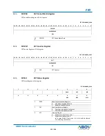
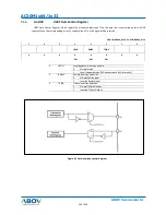
Un.BFR 

Baud rate Fraction Counter Register 

9.3.9

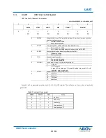
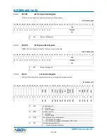
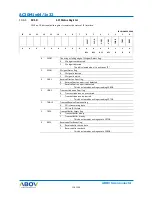
Baud rate Fraction Counter Register is 8-bit register. 

U0.BFR=0x4000_8024, U1.BFR=0x4000_8124 

BFR 

0x00 

RW 


BFR 

Fractions counter value. 

Fraction counter is disabled 

Fraction  counter  enabled.  Fraction  compensation  mode  is 

operating. Fraction counter is incremented by FCNT.   


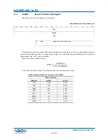
Table9.7. Example of baud rate calculation 

UART

clock

 =40 MHz 

Baud rate 

Divider 

FCNT 

Error (%) 

1200 

2083 

85 

0.00% 

2400 

1041 

170 

0.00% 

4800 

520 

213 

0.00% 

9600 

260 

106 

0.00% 

19200 

130 

53 

0.00% 

38400 

65 

262 

0.00% 

57600 

43 

103 

0.00% 

115200 

21 

179 

0.01% 


FCNT = Float ∗ 256 


FCNT value can calculated above equation. For example, the target baud rate is 4800 bps and UART

clock

 is 40MHz case, 

the BDR value is 520.8333. The integer number 520 should be the BDR value and the floating number 0.8333 will make 

the FNCT value as below. 

FCNT = 0.8333 * 256 = 213.3333, so the FCNT value is 213. 

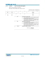
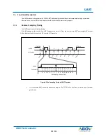
8-bit  fractional  counter  will  count  up  by  FCNT  value  every  (baud  rate)/16  periods  and  whenever  fractional  counter 

overflow  is  happen,  the  divisor  value  will  increment  by  1.  So  this  period  will  be  compensated.  Then  next  period,  the 

divisor value will return to original set value. 


Summary of Contents for AC30M1x64

Page 1: ...32 bit Cortex M0 based Programmable Motor Controller FlashROM 64 32KB SRAM 4KB AC30M1x64 AC30M1x32 USER MANUAL Version 1 1 0 2016 8 17...

Page 2: ...ment communication equipment measuring equipment domestic electrification etc Please make sure that you consult with us before you use these ABOV Semiconductor products in equipment which require high...

Page 3: ...3 246 ABOV Semiconductor INTRODUCTION SECTION 1 INTRODUCTION...

Page 4: ...4 246 4 246 AC30M1x64 1x32 ABOV Semiconductor OVERVIEW CHAPTER 1...

Page 5: ...om motor It can control up to one inverter motor Powerful and various external serial interfaces help to communicate with on board sensors and devices AC30M1x64 1x32 Block Diagram Advanced High Perfor...

Page 6: ...A14 T2IO PA13 T1IO PA12 T0IO PC8 SDA PC7 SCL T3IO PC1 SWDIO TXD1 PC0 SWCLK RXD1 VDD PC2 PC3 PC9 CLKO PC11 T0IO BOOT PC15 TXD0 PC14 RXD0 GND AN8 T2IO T0IO PA8 AN9 T1IO T3IO PA9 AN10 PA10 AN11 PA11 nRES...

Page 7: ...O AN1 PA0 T2IO AN0 PC8 SDA PC7 SCL T3IO PC1 SWDIO TXD1 PC0 SWCLK RXD1 PC11 T0IO BOOT PC14 RXD0 PB0 MPWMUH SS PB1 MPWMUL SCK PC15 TXD0 AN8 T2IO T0IO PA8 AN9 T1IO T3IO PA9 nRESET PC10 AVDD VDD AGND GND...

Page 8: ...PA1 T3IO AN1 PA0 T2IO AN0 PC8 SDA PC7 SCL T3IO PC1 SWDIO TXD1 PC0 SWCLK RXD1 PC11 T0IO BOOT PC14 RXD0 PB0 MPWMUH SS PB1 MPWMUL SCK PC15 TXD0 AN8 T2IO T0IO PA8 AN9 T1IO T3IO PA9 nRESET PC10 AVDD VDD A...

Page 9: ...n 10 ch 32 Pin Timer 16 Bit 4 ch Free Run Timer 32 Bit 1 ch Watchdog Timer 32 Bit 1 ch External communication ports 2 ch UARTs 1 ch I 2 C 1 ch SPI Hardware Divider DIV64 On Chip RC Oscillator HSI 40MH...

Page 10: ...UART SPI I2C MPWM ADC I O Ports Package AC30M1464LBN 64KB 4KB 2 1 1 1 1 unit 12 ch 44 LQFP 48 AC30M1364LBN 64KB 4KB 2 1 1 1 1 unit 10 ch 30 LQFP 32 AC30M1364UB 64KB 4KB 2 1 1 1 1 unit 10 ch 30 QFN 32...

Page 11: ...D Converter CRC CCITT UART0 UART1 I2C HSI 40MHz LSI 40kHz Clock Control MOSC 4 16MHz SOSC 32 768kHz SPI Watch Dog Timer Free Run Timer 16 Bit Timer 0 16 Bit Timer 1 16 Bit Timer 2 16 Bit Timer 3 MPWM...

Page 12: ...o be performed without the overhead of state saving and restoring 64 32KB Internal Code Flash Memory The AC30M1x64 1x32 provides internal 64 32KB code flash memory and its controller This is enough to...

Page 13: ...nication The master and the slave mode are supported Universal Asynchronous Receiver Transmitter UART The AC30M1x64 1x32 has 2 channels UART block For accurate baud rate control the fractional baud ra...

Page 14: ...ection Input signal 7 5 PB5 IOUS PORT B Bit 5 Input Output MPWMWL O MPWM WL Output 8 6 PB4 IOUS PORT B Bit 4 Input Output MPWMWH O MPWM WH Output 9 7 PB3 IOUS PORT B Bit 3 Input Output MPWMVL O MPWM V...

Page 15: ...ut AIN1 IA Analog Input 1 31 20 PA2 IOUS PORT A Bit 2 Input Output SS I O SPI Channel Slave Select In Out WDTO O Watchdog Timer Overflow Output AIN2 IA Analog Input 2 32 21 PA3 IOUS PORT A Bit 3 Input...

Page 16: ...stal Oscillator Input 46 1 PD3 IOUS PORT D Bit 3 Input Output MISO I O SPI Channel Master In Slave Out SDA I O I 2 C Channel SDA In Out SXIN I External Crystal Sub Oscillator Input 47 2 PD2 IOUS PORT...

Page 17: ...I2C ADC 0x4000 C000 0x0000 0000 MIRROR CODE 0x2000 0000 0x4000 0000 0x6000 0000 0x8000 0000 0xA000 0000 0xC000 0000 0xE000 0000 0xFFFF FFFF SRAM 4KB Peripherals Reserved Cortex M0 Peripherals 0xE010 0...

Page 18: ...18 246 18 246 ABOV Semiconductor AC30M1x64 1x32 CPU CHAPTER 2...

Page 19: ...Semiconductor CPU Cortex M0 Core 2 1 CPU core is supported from the ARM Cortex M0 processor which provides a high performance low cost platform Document DDI0432C from ARM provides detail information o...

Page 20: ...000_002C SVCall Handler 4 0x0000_0030 Debug Monitor Handler 3 0x0000_0034 Reserved 2 0x0000_0038 PenSV Handler 1 0x0000_003C SysTick Handler 0 0x0000_0040 LVDFAIL 1 0x0000_0044 SYSCLKFAIL 2 0x0000_004...

Page 21: ...terrupt has an associated priority level register Each of them is 2 bits wide occupying the two MSBs of the Interrupt Priority Level Registers Each Interrupt Priority Level Register occupies 1 byte 8...

Page 22: ...22 246 22 246 ABOV Semiconductor AC30M1x64 1x32 Boot Mode CHAPTER 3...

Page 23: ...d SPI boot UART boot uses UART0 port and SPI boot uses SPI The pins for boot mode are listed as following Table3 1 Boot mode pin list Block Pin Name Dir Description SYSTEM nRESET PC10 I Reset Input si...

Page 24: ...Followings are sample connection diagrams of boot mode AC30M1x64 AC30M1x32 VDD nRESET BOOT RXD0 TXD0 GND RESET BOOT HOST TXD RXD GND VDD 2 2 5 5V 10k Figure 3 1 Connection diagram of UART Boot AC30M1x...

Page 25: ...OT MODE ISP Mode Connections 3 3 User can design target board using any of ISP mode port AC30M1x64 AC30M1x32 VDD nRESET SWCLK SWDIO GND nRESET E PGM SWCLK SWDIO GND VDD 2 2 5 5V 10k Figure 3 3 Connect...

Page 26: ...26 246 26 246 ABOV Semiconductor AC30M1x64 1x32 SECTION 2 PERIPHERALS...

Page 27: ...27 246 ABOV Semiconductor System Control Unit SCU SYSTEM CONTROL UNIT SCU CHAPTER 1...

Page 28: ...og blocks and operating modes Internal reset and clock signals are controlled by SCU block to maintain optimize system performance and power dissipation SCU MODE CONTROL SCU CLOCK GENERATOR POWER DOWN...

Page 29: ...R3 SCU MCCR3 SCU MCCR4 5 SCU MCCR7 SCU MCCR7 MCCRn CLK SCU SCCR 1 0 SCU SCCR 1 0 SCU SCCR 2 SCU MCCRn DIV Power down Mode Power down Mode CM0 Power down Mode Sleep Mode FCLK HCLK MCLK SCU CSCR 4 SCU C...

Page 30: ...fault system clock is feed by LSI 40kHz clock LSI is default enabled at power up sequence The other clock sources will be enabled by user controls with the LSI system clock HSI 40MHz clock can be enab...

Page 31: ...CU SCCR SOSC SCU SCCR HSI MOSC 4 16MHz SOSC 32 768KHz HSI 40MHz SCU CSCR 0xXX Disable unused clock source SCU CSCR Enable All Clock Y Y Y N N N Figure 1 3 Clock change procedure When you speed up the...

Page 32: ...the system boot Internal VDC is enabled when VDDEXT power is turn on Internal POR trigger level is 1 4V of VDDEXT voltage out level At this time boot operation is started The LSI clock is enabled and...

Page 33: ...ccurred The warm reset source is controlled by SCU RSER register and the status is appeared in SCU RSSR register The reset for each peripheral blocks is controlled by SCU PRER register The reset can b...

Page 34: ...1 b1 SCU PRER1 2 WDT RESETn 1 b1 SCU PRER1 3 PCU RESETn SCU PER1 4 SCU PRER1 5 DIV RESETn SCU PER1 8 SCU PRER1 8 GPIOA RESETn SCU PER1 9 SCU PRER1 9 GPIOB RESETn SCU PER1 10 SCU PRER1 10 GPIOC RESETn...

Page 35: ...used as the low power consumption mode The low power consumption is achieved by halting processor core and unused peripherals Figure 1 7 shows the operation mode transition diagram INIT RUN SLEEP POW...

Page 36: ...6 246 AC30M1x64 1x32 ABOV Semiconductor RUN Mode 1 3 5 This mode is to operate the CPU and the peripheral hardware by using the high speed clock After reset followed by INIT state it is entered into R...

Page 37: ...ode Each peripheral function can be enabled by the function enable and clock enable bit in the PER and PCER register SLEEP MODE ENTER END WFI ENTER SLEEP MODE Wait for Interrupt signal WAKE UP SCB SCR...

Page 38: ...TRIM MODE SCU VDCCON 25 STOP2 FM MR 7 0 0x00 STOP2 SCU LVDCON 0 LVD_DISABLE SETUP WAKE UP SOURCE SCU CSCR Enable All Clock Wait for stabilizing SCU SCCR LSI SCU CSCR 0x20 only LSI enable SCB SCR 2 1...

Page 39: ...PIN DESCRIPTION 1 4 Table 1 3 SCU pins PIN NAME TYPE DESCRIPTION nRESET I External Reset Input XIN XOUT OSC External Crystal Oscillator SXIN SXOUT OSC External sub Crystal Oscillator STBO O Stand by O...

Page 40: ...clock enable register 1 0000_000F PCER2 0x0034 RW Peripheral clock enable register 2 0000_0101 CSCR 0x0040 RW Clock Source Control register 0000_0020 SCCR 0x0044 RW System Clock Control register 0000_...

Page 41: ...de 1 VDC isn t automatically off entering power down mode 5 4 PREVMODE Previous operating mode before current reset event 00 Previous operating mode was RUN mode 01 Previous operating mode was SLEEP m...

Page 42: ...e wakeup source of GPIOD port pin change event 0 Not used for wakeup source 1 Enable the wakeup event generation 10 GPIOCWUE Enable wakeup source of GPIOC port pin change event 0 Not used for wakeup s...

Page 43: ...Status of wakeup source of GPIOD port pin change event 0 No wakeup event 1 Wakeup event was generated 10 GPIOCWU Status of wakeup source of GPIOC port pin change event 0 No wakeup event 1 Wakeup even...

Page 44: ...sked 1 Reset from this event is enabled 6 PINRST External pin reset enable bit 0 Reset from this event is masked 1 Reset from this event is enabled 5 CPURST CPU request reset enable bit 0 Reset from t...

Page 45: ...bit 0 Read Reset from this event was not exist Write no effect 1 Read Reset from this event was occurred Write Clear the status 5 CPURST CPU request reset status bit 0 Read Reset from this event was...

Page 46: ...19 18 17 16 15 14 13 12 11 10 9 8 7 6 5 4 3 2 1 0 FRT TIMER3 TIMER2 TIMER1 TIMER0 GPIOD GPIOC GPIOB GPIOA DIV64 PCU WDT FMC SCU 0 0 0 0 0 1 0 0 0 0 0 0 1 1 1 1 0 0 0 0 1 1 1 1 0 0 1 0 1 1 1 1 RW RW R...

Page 47: ...4000_0024 31 30 29 28 27 26 25 24 23 22 21 20 19 18 17 16 15 14 13 12 11 10 9 8 7 6 5 4 3 2 1 0 ADC MPWM UART1 UART0 I2C SPI 0 0 0 0 0 0 0 0 0 0 0 1 0 0 0 1 0 0 0 0 0 0 1 1 0 0 0 1 0 0 0 1 RW RW RW RW...

Page 48: ...1 0x4000_0028 31 30 29 28 27 26 25 24 23 22 21 20 19 18 17 16 15 14 13 12 11 10 9 8 7 6 5 4 3 2 1 0 FRT TIMER3 TIMER2 TIMER1 TIMER0 GPIOD GPIOC GPIOB GPIOA DIV64 Reserved Reserved Reserved Reserved 0...

Page 49: ...29 28 27 26 25 24 23 22 21 20 19 18 17 16 15 14 13 12 11 10 9 8 7 6 5 4 3 2 1 0 ADC MPWM UART1 UART0 I2C SPI 0 0 0 0 0 0 0 0 0 0 0 0 0 0 0 0 0 0 0 0 0 0 0 1 0 0 0 0 0 0 0 1 RW RW RW RW RW RW 20 ADC A...

Page 50: ...stopped PCER1 0x4000_0030 31 30 29 28 27 26 25 24 23 22 21 20 19 18 17 16 15 14 13 12 11 10 9 8 7 6 5 4 3 2 1 0 FRT TIMER3 TIMER2 TIMER1 TIMER0 GPIOD GPIOC GPIOB GPIOA DIV64 Reserved Reserved Reserve...

Page 51: ...respond PCER2 0x4000_0034 31 30 29 28 27 26 25 24 23 22 21 20 19 18 17 16 15 14 13 12 11 10 9 8 7 6 5 4 3 2 1 0 ADC MWPM UART1 UART0 I2C SPI 0 0 0 0 0 0 0 0 0 0 0 0 0 0 0 0 0 0 0 0 0 0 0 1 0 0 0 0 0 0...

Page 52: ...rnal oscillator divide by 2 3 2 HSICON High speed internal oscillator control 0X Disable high speed internal oscillator 10 Enable high speed internal oscillator 11 Enable high speed internal oscillato...

Page 53: ...cillator fail interrupt is pending Write Clear pending interrupt 8 SOSCSTS External sub oscillator status 0 Not oscillate 1 External sub oscillator is working normally 7 MCLKMNT MCLK monitoring enable...

Page 54: ...2 PROTSTS Protection condition status bit This bit can t invoke NMI interrupt without enable bit 0 Not occurred 1 Event occurred 11 OVPSTS Over Voltage Protection condition status bit This bit can t i...

Page 55: ...st divider To use CLKO output function it should be set as CLKO that has output mode in Pin Mux Clock Output Register is 8 bit register COR 0x4000_0050 7 6 5 4 3 2 1 0 CLKOEN CLKODIV 000 0 1111 RO RW...

Page 56: ...E VDCMODE value write enable Write only with VDCMODE value 0 VDCMODE field is not updated by writing 1 VDCMODE filed can be updated by writing 25 STOPSEL STOP MODE Select bit 0 VDC STOP MODE 1 1 VDC S...

Page 57: ...te enable Write only 0 LVDSEL field is not updated by writing 1 LVDSEL filed can be updated by writing 9 8 LVDSEL LVD detect level select 00 LVD detect level is 1 73V 01 LVD detect level is 2 65V 10 L...

Page 58: ...0 0 RW RW 31 BISCON Build in self calibration function enable 0 BISC function disabled IOSC supplies factory calibrated frequency 1 BISC function enabled IOSC supplies self calibrated frequency 30 REF...

Page 59: ...4 23 22 21 20 19 18 17 16 15 14 13 12 11 10 9 8 7 6 5 4 3 2 1 0 INTOSC_COMP XTAL_COMP 0 0 RW RW 31 16 INTOSC_COMP 31 16 INTOSC compare value 15 0 XTAL_COMP 15 0 XTAL Compare value Calibration supports...

Page 60: ...KEN 0 0 0 0 WO RW WO RW 15 FILSKIPWEN Write enable of bit field FILSKIPEN 0 Write access of FILSKIPEN field is masked 1 Write access of FILSKIPEN field is accepted 8 FILSKIPEN Control External Main Os...

Page 61: ...e Status Register 1 5 23 External Mode Status Register shows external mode pin status while booting This register is 8 bit register EMODR 0x4000_0084 7 6 5 4 3 2 1 0 Reserved Reserved BOOT 0x0 RO RO 0...

Page 62: ...SYSTICK external clock source This register is 32 bit register MCCR1 0x4000_0090 31 30 29 28 27 26 25 24 23 22 21 20 19 18 17 16 15 14 13 12 11 10 9 8 7 6 5 4 3 2 1 0 Reserved Reserved Reserved STCSEL...

Page 63: ...ed MPWM it must set this register This register is 32 bit register MCCR2 0x4000_0094 31 30 29 28 27 26 25 24 23 22 21 20 19 18 17 16 15 14 13 12 11 10 9 8 7 6 5 4 3 2 1 0 Reserved Reserved PWMCSEL PWM...

Page 64: ...31 30 29 28 27 26 25 24 23 22 21 20 19 18 17 16 15 14 13 12 11 10 9 8 7 6 5 4 3 2 1 0 TIMERCSEL TIMERDIV WDTCSEL WDTDIV 0 0 0 0 0 000 0x01 0 0 0 0 0 000 0x01 RW RW RW RW 26 24 TIMERCSEL Timer Clock so...

Page 65: ...11 10 9 8 7 6 5 4 3 2 1 0 PBDCSEL PBDDIV PADCSEL PADDIV 0 0 0 0 0 000 0x01 0 0 0 0 0 000 0x01 RW RW RW RW 26 24 PBDCSEL Debounce Clock for Port B source select bit 000 LSI 100 MCLK 101 HSI 110 MOSC 11...

Page 66: ...1 10 9 8 7 6 5 4 3 2 1 0 PDDCSEL PDDDIV PCDCSEL PCDDIV 0 0 0 0 0 000 0x01 0 0 0 0 0 000 0x01 RW RW RW RW 26 24 PDDCSEL Debounce Clock for PORT D source select bit 000 LSI 100 MCLK 101 HSI 110 MOSC 111...

Page 67: ..._00A8 31 30 29 28 27 26 25 24 23 22 21 20 19 18 17 16 15 14 13 12 11 10 9 8 7 6 5 4 3 2 1 0 ADCCSEL ADCCDIV UARTCSEL UARTCDIV 0 0 0 0 0 000 0x01 000 0x01 RW RW RW RW 26 24 ADCCSEL ADC clock source sel...

Page 68: ...be changed until the frequency of INTOSC cross the target frequency level 8 steps up trim and 8 steps down trim are available with 0 7 difference in each step Update period is decided by reference cl...

Page 69: ...69 246 ABOV Semiconductor Port Control Unit PCU PORT CONTROL UNIT PCU CHAPTER 2...

Page 70: ...rnal I Os as below Set pin function mux Set external signal directions of each pins Set interrupt trigger mode for each pins Set internal pull up register control and open drain control PORT CONTROL F...

Page 71: ...bounce count Pull up Enable Analog input AN0 AN11 XIN XOUT SXIN SXOUT VDDIO VDDIO PIN Figure 2 2 I O Port Block Diagram ADC and External Oscillator pins Open drain Enable Input mode 00 01 10 11 Port M...

Page 72: ...1 PA1 T3IO AIN1 2 PA2 SS WDTO AIN2 3 PA3 SCK STBO AIN3 4 PA4 AIN4 5 PA5 AIN5 6 PA6 T0IO AIN6 7 PA7 T1IO AIN7 8 PA8 T2IO T0IO AIN8 9 PA9 T3IO T1IO AIN9 10 PA10 AIN10 11 PA11 AIN11 12 PA12 T0IO 13 PA13...

Page 73: ...2 PC2 3 PC3 4 PC4 T0IO 5 PC5 RXD1 T1IO 6 PC6 TXD1 T2IO 7 PC7 SCL T3IO 8 PC8 SDA VMRG 9 PC9 CLKO 10 PC10 nRESET 11 PC11 BOOT T0IO 12 PC12 T3IO XIN 13 PC13 T2IO XOUT 14 PC14 RXD0 15 PC15 TXD0 PD 0 PD0 S...

Page 74: ...ESS PCA 0x4000_1000 PCB 0x4000_1100 PCC 0x4000_1200 PCD 0x4000_1300 Table 2 4 PCU Register map NAME OFFSET TYPE DESCRIPTION PCn MR 0x 00 RW Port n pin mux select register PCn CR 0x 04 RW Port n pin co...

Page 75: ...11 10 9 8 7 6 5 4 3 2 1 0 PA15 PA14 PA13 PA12 PA11 PA10 PA9 PA8 PA7 PA6 PA5 PA4 PA3 PA2 PA1 PA0 00 00 00 00 00 00 00 00 00 00 00 00 00 00 00 00 RW RW RW RW RW RW RW RW RW RW RW RW RW RW RW RW PORT SEL...

Page 76: ...0x4000_1100 31 30 29 28 27 26 25 24 23 22 21 20 19 18 17 16 15 14 13 12 11 10 9 8 7 6 5 4 3 2 1 0 PB15 PB14 PB13 PB12 PB11 PB10 PB9 PB8 PB7 PB6 PB5 PB4 PB3 PB2 PB1 PB0 00 00 00 00 00 00 00 00 00 00 00...

Page 77: ...5 14 13 12 11 10 9 8 7 6 5 4 3 2 1 0 PC15 PC14 PC13 PC12 PC11 PC10 PC9 PC8 PC7 PC6 PC5 PC4 PC3 PC2 PC1 PC0 00 00 00 00 01 01 00 00 00 00 00 00 00 00 01 01 RW RW RW RW RW RW RW RW RW RW RW RW RW RW RW...

Page 78: ...arantee its functionality PCD MR 0x4000_1300 31 30 29 28 27 26 25 24 23 22 21 20 19 18 17 16 15 14 13 12 11 10 9 8 7 6 5 4 3 2 1 0 PD15 PD14 PD13 PD12 PD11 PD10 PD9 PD8 PD7 PD6 PD5 PD4 PD3 PD2 PD1 PD0...

Page 79: ...ch port pin Each pin can be configured as input pin output pin or open drain pin PCC CR 0x4000_1204 31 30 29 28 27 26 25 24 23 22 21 20 19 18 17 16 15 14 13 12 11 10 9 8 7 6 5 4 3 2 1 0 P15 P14 P13 P1...

Page 80: ...E15 PDE14 PDE13 PDE12 PDE11 PDE10 PDE9 PDE8 PDE7 PDE6 PDE5 PDE4 PDE3 PDE2 PDE1 PDE0 0000 RW PDEn Pin debounce enable 0 Disable debounce filter 1 Enable debounce filter PCn IER PORT n Interrupt Enable...

Page 81: ...dge interrupt event is present 10 High level interrupt or rising edge interrupt event is present 11 Both of rising and falling edge interrupt event is present in edge trigger interrupt mode Not availa...

Page 82: ...000_1FF0 15 14 13 12 11 10 9 8 7 6 5 4 3 2 1 0 PORTEN 0 0 0 0 0 0 0 0 WO 7 0 PORTEN Writing the sequence of 0x15 and 0x51 in this register enables writing to PCU registers and writing other values pro...

Page 83: ...C 3 IN Control logic Pin Control register VDDIO PAD R W R W R W R W VDDIO OUTPUT CONTROL LOGIC INPUT CONTROL LOGIC AIN5V 200 Ohm 200 Ohm Figure 2 4 Functional Bloack diagram When the input functions o...

Page 84: ...each port group used by MCCR4 5 Register 2 bit UP DOWN Counter External Input PORT in UP 1 DOWN 0 FF CNT 1 0 CLK Debounce Clock Internal Input CNT 1 0 01 1 CNT 1 0 10 0 Counter operation If PORT In 1...

Page 85: ...85 246 ABOV Semiconductor General Purpose I O GPIO GENERAL PURPOSE I O GPIO CHAPTER 3...

Page 86: ...of pins except dedicated function pins can be used general I O ports General input output ports are controlled by GPIO block Output signal level H L select Read Input signal level Pn BSR Pn BCR Pn ODR...

Page 87: ...87 246 ABOV Semiconductor General Purpose I O GPIO Pin description 3 2 Table 3 1 External signal PIN NAME TYPE DESCRIPTION PA IO PA0 PA15 PB IO PB0 PB7 PC IO PC0 PC15 PD IO PD0 PD3...

Page 88: ...ort NAME BASE ADDRESS PA PORT 0x4000_2000 PB PORT 0x4000_2100 PC PORT 0x4000_2200 PD PORT 0x4000_2300 Table 3 3 GPIO Register map NAME OFFSET TYPE DESCRIPTION RESET VALUE Pn ODR 0x 00 RW Port n Output...

Page 89: ...6 5 4 3 2 1 0 ODR 0000 RW ODR Pin output level 0 Output low level 1 Output high level Pn IDR PORT n Input Data Register 3 3 2 Each pin level status can be read in the Pn IDR register Even if the pin...

Page 90: ...13 12 11 10 9 8 7 6 5 4 3 2 1 0 BSR 0000 WO BSR Pin current level 0 Not effect 1 Set correspondent bit in Pn ODR register Pn BCR PORT n Bit Clear Register 3 3 4 Pn BCR is a register for control each b...

Page 91: ...NTROL UNIT GPIO BLOCK Figure 3 2 Functional Block diagram When configured as output the value written to the GPIO Output Data Register is output on the I O Pin When set the Bit Set Register GPIO Outpu...

Page 92: ...92 246 92 246 AC30M1x64 1x32 ABOV Semiconductor FLASH MEMORY CONTROLLER CHAPTER 4...

Page 93: ...er 20MHz 1 wait 2 wait and pre fetch read acceleration access support Use internal 40MHz OSC clock to make timing control for Erase Program Start address FLASH MEMORY 64KB 0x0000_0000 0x0000_1000 0x00...

Page 94: ...ry Control register 0x05000000 FM AR 0x000C RW Flash Memory Address register 0x00000000 FM DR 0x0010 RW Flash Memory Data register 0x00000000 FM TMR 0x0014 RW Flash Memory Timer register 0x00018FFF FM...

Page 95: ...register enable 0 means can set TEST reg 22 AMBAEN 0 AMBA mode disabled status 1 AMBA mode enable can change wait state and etc 21 PROTEN 0 Flash protection register disable 0 means cannot access prot...

Page 96: ...1 OTP area 1 access enable user can access in a certain condition OTP1 is used for read protection 28 OTP0 0 1 OTP area 0 access enable user can not erase program this area 20 TMREN 0 Flash Tick timer...

Page 97: ...97 246 ABOV Semiconductor Flash Memory Controller 1 Write enable 3 PBLD 0 1 Page buffer load WE should be set 2 PGM 0 1 Program mode enable 1 ERS 0 1 Erase mode enable 0 PBR 0 1 Page buffer reset...

Page 98: ...program data register FM DR 0x4000_0110 31 30 29 28 27 26 25 24 23 22 21 20 19 18 17 16 15 14 13 12 11 10 9 8 7 6 5 4 3 2 1 0 FDATA 0x0000_0000 RW 31 0 FDATA Flash PGM data 32 bit FM TMR Flash Memory...

Page 99: ...0x3FFFF from written TICK value while TMR runs by PCLK clock while Flash PGM or ERS counts up only when IDLE bit of FMMR register is low FM CRC Flash CRC check register 4 2 7 FMCRC is the CRC value re...

Page 100: ...STCLK 0 TEST Clock selection test purpose only Set 1 to use system bus clock instead of internal 40MHz OSC This bits only be written in AMBA mode and MSB 16 bit bit 31 16 must be 0x7858 9 8 WAIT This...

Page 101: ...ister is 32 bit read only register FM HWID 0x4000_0140 31 30 29 28 27 26 25 24 23 22 21 20 19 18 17 16 15 14 13 12 11 10 9 8 7 6 5 4 3 2 1 0 FHWID 0x3014_6400 R 31 0 FHWID Flash HWID register It retur...

Page 102: ...e when AMBA mode is enabled FM MR 0x81 FM MR 0x28 AMBA mode enter change BOOTCR 4 SREMAP value FM MR 0 AMBA mode exit FM WPROT Flash Memory Write Protection Register 4 2 11 Internal flash memory write...

Page 103: ...SRAM or debugger 0xA5A5A5A5 will be return as read data LOCK2 Read protection level 2 Code protection mode enable debug cannot be connected Write any value except 0x39 include 0xFF to activate LOCK2 o...

Page 104: ...PMODE bit of FM CR J Clear Flash mode write 0x00 into FM MR K Insert at least 2 NOPs and return to normal operation 3 Program example include page buffer load A Flash mode enable to write FM CR regist...

Page 105: ...105 246 ABOV Semiconductor Internal SRAM INTERNAL SRAM CHAPTER 5...

Page 106: ...is 4KB The SRAM base address is 0x2000_0000 The SRAM memory area is usually used for data memory and stack memory Sometimes the code is dumped into the SRAM memory for fast operation or flash erase pg...

Page 107: ...107 246 ABOV Semiconductor Watch Dog Timer WATCH DOG TIMER WDT CHAPTER 6...

Page 108: ...down counter WDT CNT Select reset or periodic interrupt Count clock selection Dedicated pre scaler Watchdog underflow output signal APB interface WDT_RESETn WDTRE WDT CON 6 WDT LOGIC WUF WDT CON 8 WDT...

Page 109: ...write into WDTLR register with target value of WDTCNT It needs at least 5 WDT clocks to update WDTLR to WDTCNT WDT ext clock source is controlled by WDTCSEL and WDTDIV in MCCR3 WDT LR 0x4000_0200 31...

Page 110: ...g when debug mode 1 Watchdog counter stopped when debug mode 8 WUF Watchdog timer underflow flag 0 No underflow 1 Underflow is pending 7 WDTIE Watchdog timer counter underflow interrupt enable 0 Disab...

Page 111: ...WDT CON It takes up to 5 cycles from Load value to the CNT value The WDT interrupt signal and CNT value data might be delayed maximum by 2 system bus clocks in synchronous logic Prescale Table 6 3 2 T...

Page 112: ...4 WDTCLKIN 128 WDTCLKIN 256 LSI 40kHz 10kHz 5kHz 2 5kHz 1 25kHz 0 625kHz 0 3125kHz 0 15625kHz MCLK Bus clock MCLK 4 MCLK 8 MCLK 16 MCLK 32 MCLK 32 MCLK 128 MCLK 256 HSI 40MHz 10MHz 5MHz 2 5MHz 1 25MHz...

Page 113: ...113 246 ABOV Semiconductor 16 bit Timer 16 BIT TIMER CHAPTER 7...

Page 114: ...t periodic timer PWM pulse one shot timer and capture mode They can be synchronized together One more optional free run timer is provided The main purpose of this timer is a periodical tick timer or a...

Page 115: ...115 246 ABOV Semiconductor 16 bit Timer Pin description 7 2 Table 7 1 External pin PIN NAME TYPE DESCRIPTION TnIO I O External clock capture input and PWM one shot output...

Page 116: ...mer Register Map NAME OFFSET TYPE DESCRIPTION RESET VALUE Tn CR1 0x 00 RW Timer control register 1 0x00000000 Tn CR2 0x 04 RW Timer control register 2 0x00000000 Tn PRS 0x 08 RW Timer prescaler regist...

Page 117: ...unter with other synchronized timers 0 Single counter mode 1 Synchronized counter clear mode 13 UAO Select GRA GRB update mode 0 Writing GRA or GRB takes effect after current period 1 Writing GRA or G...

Page 118: ...register This bit will be cleared after next timer clock 0 TEN Timer enable bit 0 Stop timer counting 1 Start timer counting Note It is recommended to start timer with TCLR bit setting to be 1 Tn PRS...

Page 119: ...ng edge of TnIO port will capture the count value when falling edge clear mode Tn GRB Timer n General Register B 7 3 5 Timer General Register B is 16 bit register T0 GRB 0x4000_3010 T1 GRB 0x4000_3030...

Page 120: ...irst count 0xFF Prescaler will not be initialized and maintain current conditions even writing timer count value on Tn CNT 15 0 First count period is not accurate depends on its status when writing op...

Page 121: ...n correspondent bit in the Tn IER register T0 IER 0x4000_301C T1 IER 0x4000_303C T2 IER 0x4000_305C T3 IER 0x4000_307C 7 6 5 4 3 2 1 0 MAIE MBIE OVIE 0 0 0 0 0 0 0 0 RW RW RW 2 MAIE GRA Match interrup...

Page 122: ...ation The period of timer count can be calculated as below equation The period TMCLK Period Tn GRB value Match A interrupt time TMCLK Period Tn GRA value If Tn CR1 UAO bit is 0 Tn CR2 TCLR command wil...

Page 123: ...B 0 the timer cannot be started even Tn CR2 TEN is 1 That s because the period is 0 The value in Tn GRA and Tn GRB is loaded into internal compare data buffer 0 and 1 when the loading condition is occ...

Page 124: ...Tn GRB 0 the timer cannot be started even Tn CR2 TEN is 1 Because the period is 0 The value in Tn GRA and Tn GRB is loaded into internal compare data buffer 0 and 1 when the loading condition is occu...

Page 125: ...fer 0 and 1 when the loading condition is occurred In this periodic mode with Tn CR1 UAO 0 Tn CR2 TCLR write operation will load the data buffer and the next GRB match event will load the data buffer...

Page 126: ...A T0 CNT T0 GRB T1 CNT T1 GRB For timing synchronization every GRB register should have same values T0 GRB T0 GRA T1 CR2 TEN 1 T1 CNT Timer0 was cleared by start event of Timer1 Timer0 restarts Timer0...

Page 127: ...apture the counter valued in each capture conditions Figure 7 8 Capture mode timing diagram 5 PCLK clock cycle is required internally So actual capture point is after 5 PCLK clock cycles from rising o...

Page 128: ...128 246 128 246 ABOV Semiconductor AC30M1x64 1x32 Figure 7 9 ADC trigger function timing diagram...

Page 129: ...129 246 ABOV Semiconductor FRT FREE RUN TIMER FRT CHAPTER 8...

Page 130: ...ck is a 32 bit Free Run Timer It can be used in Power down Mode 32 bit up counter with SOSC MOSC LSI Matched Interrupt APB LSI CLK MOSC CLK SOSC CLK FRT 00 01 10 32 DIVIDER FRT MR 5 4 32 Bit FRT CNT F...

Page 131: ...channel NAME BASE ADDRESS FRT 0x4000_0600 Table 8 2 FRT register map NAME OFFSET TYPE DESCRIPTION RESET VALUE FRT MR 0x0000 RW FRT mode register 0x00000000 FRT CR 0x0004 RW FRT control register 0x000...

Page 132: ...Whenever the counter matches FRT PER the counter will be set zero and waiting for MF to be cleared 1 Counter Match Clear function is disabled The counter will keep countering without set zero 1 OVIE O...

Page 133: ...22 21 20 19 18 17 16 15 14 13 12 11 10 9 8 7 6 5 4 3 2 1 0 CNT 0x0000_0000 RO 32 0 CNT FRT Counter FRT SR FRT Status Register 8 2 5 FRT Status Register is 8 bit register FRT SR 0x4000_0610 7 6 5 4 3 2...

Page 134: ...134 246 134 246 ABOV Semiconductor AC30M1x64 1x32 FUNCTION DESCRIPTION 8 3...

Page 135: ...135 246 UART ABOV Semiconductor UNIVERSAL ASYNCHRONOUS CHAPTER 9 RECEIVER TRANSMITTER UART...

Page 136: ...ternally divided by 16 of the prescaled clock and 8 bit precision clock tuning function Programmable interrupt generation function will help to control the communication via UART channel Compatible wi...

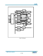
Page 137: ...R TRANSMITTER HOLDING REGISTER INTERRUPT ENABLE REGISTER BAUD GENERATOR TRNASMITTER TIMING CONTROL TRANSMITTER BUFFER RECEIVER TIMING CONTROL RECEIVER BUFFER DIVISOR LATCH LSB DIVISOR LATCH MSB BFR Fr...

Page 138: ...Semiconductor Pin description 9 2 Table 9 1 External signal PIN NAME TYPE DESCRIPTION TXD0 O UART Channel 0 transmit output RXD0 I UART Channel 0 receive input TXD1 O UART Channel 1 transmit output R...

Page 139: ...R 0x0C RW Line control register 0x00 Un DCR 0x10 RW Data Control Register Un LSR 0x14 R Line status register 0x00 0x18 reserved Un SCR 0x1C RW Scratch pad register 0x00 Un BDR 0x20 RW Baud rate Diviso...

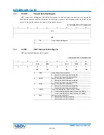
Page 140: ...ister U0 IER 0x4000_8004 U1 IER 0x4000_8104 7 6 5 4 3 2 1 0 TXIEN RXIEN RLSIE THREIE DRIE 0 0 0 0 0 0 0 0 RW RW RW RW RW 5 TXIEN Transmit done interrupt enable 0 Receive line status interrupt is disab...

Page 141: ...empty flag 16 DR Data receive interrupt flag 4 TXE Interrupt source ID See interrupt source ID table 3 1 IID Interrupt source ID See interrupt source ID table 0 IPEN Interrupt pending bit 0 Interrupt...

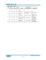
Page 142: ...1 0 Receiver Line Status Overrun Parity Framing or Break Error Read LSR register 2 0 1 0 0 Receiver Data Available Receive data is available Read receive register or read IIR register 3 0 0 1 0 Trans...

Page 143: ...ITY 4 PARITY Parity mode selection bit and stuck parity select bit 0 Odd parity mode 1 Even parity mode 3 PEN Parity bit transfer enable 0 The parity bit disabled 1 The parity bit enabled 2 STOPBIT Th...

Page 144: ...ata line of Tx or RX signal will be inverted U0 DCR 0x4000_8010 U1 DCR 0x4000_8110 7 6 5 4 3 2 1 0 LBON RXINV TXINV 0 0 0 0 0 0 0 0 RW RW RW 4 LBON Local loopback test mode enable 0 Normal mode 1 Loca...

Page 145: ...error The receive character did not have a valid stop bit 2 PE Parity Error 0 No parity error 1 Parity error The receive character does not have correct parity information 1 OE Overrun error 0 No ove...

Page 146: ...be set properly The programmable baud rate generate is provided to give from 1 to 65535 divider number The 16 bit divider register UnBDR should be written for expected baud rate UARTclock gets from M...

Page 147: ...800 520 213 0 00 9600 260 106 0 00 19200 130 53 0 00 38400 65 262 0 00 57600 43 103 0 00 115200 21 179 0 01 FCNT Float 256 FCNT value can calculated above equation For example the target baud rate is...

Page 148: ...ingle sample will be done at 8 16 baud rate for the start bit 1 Multi sampling is enabled for start bit Sampling is done 3 times at 7 16 8 16 and 9 16 baud rate Dominant value of 3 samples will be sel...

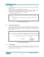
Page 149: ...ates as following timing If the falling edge on the receive line UART judges as the start bit From the start timing UART oversamples 16 times of 1 bit and detect the bit value at the 7th sample of 16...

Page 150: ...data format is below Figure 9 4 Transmit data format example Inter frame delay transmission 9 4 3 The inter frame delay function allows the transmitter to insert an idle state on the TXD line between...

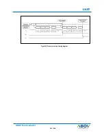
Page 151: ...151 246 ABOV Semiconductor UART Figure 9 6 Transmit interrupt timing diagram...

Page 152: ...152 246 152 246 ABOV Semiconductor AC30M1x64 1x32 SERIAL PERIPHERAL INTERFACE SPI CHAPTER 10...

Page 153: ...eration Programmable clock polarity and phase 8 9 16 17 bit wide transmit receive register 8 9 16 17 bit wide data frame Loop back mode Programmable start burst and stop delay time SPI Register Block...

Page 154: ...PIN DESCRIPTION 10 2 Table 10 1 External Pins PIN NAME TYPE DESCRIPTION SS I O SPI Slave select input output SCK I O SPI Serial clock input output MOSI I O SPI Serial data Master output Slave input M...

Page 155: ...00_9000 Table 10 3 SPI Register Map NAME OFFSET TYPE DESCRIPTION RESET VALUE SP TDR 0x00 W SPI Transmit Data Register SP RDR 0x00 R SPI Receive Data Register 0x000000 SP CR 0x04 RW SPI Control Registe...

Page 156: ...0 0 0 0 0 0 0x00000 RW 16 0 RDR Receive Data Register SP CR SPI Control Register 10 3 3 SP CR is a 20 bits read write register and can be set to configure SPI operation mode SP CR 0x4000_9004 31 30 29...

Page 157: ...ct bit 0 SS output signal is disabled 1 SS output signal is enabled 8 SSPOL SS signal Polarity select bit 0 SS signal is Active Low 1 SS signal is Active High 5 MS Master Slave select bit 0 SPI is in...

Page 158: ...s inactive 1 SS signal is active 4 OVRF Receive Overrun Error flag 0 Receive Overrun error is not detected 1 Receive Overrun error is detected This bit is cleared by writing or reading SP RDR 3 UDRF T...

Page 159: ...Register 10 3 5 SP BR is an16 bits read write register Baud rate can be set by writing the register SP BR 0x4000_900C 15 14 13 12 11 10 9 8 7 6 5 4 3 2 1 0 BR 0x00FF RW 15 0 BR Baud rate setting bits...

Page 160: ...P EN 0x4000_9010 7 6 5 4 3 2 1 0 ENABLE 0 0 0 0 0 0 0 0 RW 0 ENABLE SPI Enable bit 0 SPI is disabled SP SR is initialized by writing 0 to this bit but other registers aren t initialized 1 SPI is enabl...

Page 161: ...27 26 25 24 23 22 21 20 19 18 17 16 15 14 13 12 11 10 9 8 7 6 5 4 3 2 1 0 SPL BTL STL 0 0 0 0 0 0 0 0 0x01 0x01 0x01 RW RW RW 23 16 SPL StoP Length value 0x01 0xFF 1 255 SCLKs SPL 1 15 8 BTL BursT Len...

Page 162: ...f both device master and slave The nSS line is the slave select input of the slave The nSS pin of the master is not shown in the diagrams It has to be inactive by a high level on this pin if configure...

Page 163: ...ts inactive to its active state rising edge if CPOL equals zero and falling edge if CPOL equals one causes both the master and the slave to output the MSB of the byte in the SP TDR As shown in Figure...

Page 164: ...164 246 164 246 ABOV Semiconductor AC30M1x64 1x32 I2 C Interface CHAPTER 11...

Page 165: ...ommunication speed Multi master bus configuration 7 bit addressing mode Standard data rate of 100 400 KBps STOP signal generation and detection START signal generation ACK bit generation and detection...

Page 166: ...miconductor AC30M1x64 1x32 PIN DESCRIPTION 11 2 Table 11 1 I 2 C interface external pins PIN NAME TYPE DESCRIPTION SCL I O I 2 C channel Serial clock bus line open drain SDA I O I 2 C channel Serial d...

Page 167: ...000_A000 Table 11 3 I 2 C register map NAME OFFSET TYPE DESCRIPTION RESET VALUE IC DR 0x00 RW I 2 C Data Register 0xFF IC SR 0x08 R RW I 2 C Status Register 0x00 IC SAR 0x0C RW I 2 C Slave Address Reg...

Page 168: ...ta Register 11 3 1 IC DR is an 8 bits read write register It contains a byte of serial data to be transmitted or a byte which has just been received IC DR 0x4000_A000 7 6 5 4 3 2 1 0 ICDR 0xFF RW 7 0...

Page 169: ...neral call detected or slave address ID byte was sent 6 TEND 1 Byte transmission complete flag 0 The transmission is working or not completed 1 The transmission is completed 5 STOP STOP flag 0 STOP is...

Page 170: ...ddress Register 11 3 3 IC SAR is an 8 bits read write register It shows the address in slave mode IC SAR 0x4000_A00C 7 6 5 4 3 2 1 0 SVAD GCEN 0x00 0 RW RW 7 1 SVAD 7 bit Slave Address 0 GCEN General...

Page 171: ...F Interrupt status bit 0 Interrupt is inactive 1 Interrupt is active 5 SOFTRST Soft Reset enable bit 0 Soft Reset is disabled 1 Soft Reset is enabled 4 INTEN Interrupt enabled bit 0 Interrupt is disab...

Page 172: ...3 5 IC SCLL is a 16 bit read write register SCL LOW time can be set by writing this register in master mode IC SCLL 0x4000_A018 15 14 13 12 11 10 9 8 7 6 5 4 3 2 1 0 SCLL 0xFFFF RW 15 0 SCLL SCL LOW d...

Page 173: ...is a 16 bit read write register SCL HIGH time will be set by writing this register in master mode IC SCLH 0x4000_A01C 15 14 13 12 11 10 9 8 7 6 5 4 3 2 1 0 SCLH 0xFFFF RW 15 0 SCLH SCL HIGH duration...

Page 174: ...DH is a 15 bit read write register SDA HOLD time will be set by writing this register in master mode IC SDH 0x4000_A020 15 14 13 12 11 10 9 8 7 6 5 4 3 2 1 0 SDH 0x7FFF RW 14 0 SDH SDA HOLD time setti...

Page 175: ...he data on the SDA line must be stable during the H period of the clock The H or L state of the data line can only change when the clock signal on the SCL line is L see Fig 11 6 Figure 11 6 I 2 C Bus...

Page 176: ...to be free again a certain time after the STOP condition The bus is busy if a repeated START Sr is generated instead of a STOP condition In this respect the START S and repeated START Sr conditions a...

Page 177: ...t can hold the clock line SCL L to force the master into a wait state Data transfer then continues when the slave is ready for another byte of data and releases clock line SCL A message which starts w...

Page 178: ...ate either a STOP condition to abort the transfer or a repeated START condition to start a new transfer If a slave receiver does acknowledge the slave address but sometime later in the transfer cannot...

Page 179: ...o start counting off their L period and once a device clock has gone L it will hold the SCL line in that state until the clock H state is reached see Figure 11 10 However the L to H transition of this...

Page 180: ...s determined by the winning master no information is lost during the arbitration process A master that loses the arbitration can generate clock pulses until the end of the byte in which it loses the a...

Page 181: ...riting Master Transmitter 11 5 1 It shows the flow of transmitter in master mode see Figure 11 12 Figure 11 12 Transmitter Flowchart in Master mode From master to slave Master command or Data Write Fr...

Page 182: ...ver Flowchart in Master mode From master to slave Master command or Data Write From slave to master ACK Interrupt SCL line is held low Interrupt after stop command P ACK Arbitration lost as master and...

Page 183: ...e 11 14 Transmitter Flowchart in Slave mode SLA R ACK DATA LOST S or Sr Y ACK STOP Y N P IDLE IDLE Y GCALL From master to slave Master command or Data Write From slave to master ACK Interrupt SCL line...

Page 184: ...5 Figure 11 15 Receiver Flowchart in Slave mode SLA W ACK DATA LOST S or Sr Y N ACK STOP Y N P IDLE IDLE Y GCALL From master to slave Master command or Data Write From slave to master ACK Interrupt SC...

Page 185: ...185 246 ABOV Semiconductor Motor PWM MOTOR PULSE WIDTH MODULATOR CHAPTER 12 MPWM...

Page 186: ...s mpwm counter clock source will be provided from SCU block The MPWM resolution and period will be defined by this MPWM clock configuration The default MPWM clock is same as RINGOSC clock Before enabl...

Page 187: ...TYPE DESCRIPTION MPWMUH O MPWM Phase U H side output MPWMUL O MPWM Phase U L side output MPWMVH O MPWM Phase V H side output MPWMVL O MPWM Phase V L side output MPWMWH O MPWM Phase W H side output MP...

Page 188: ...0x0024 RW MPWM Duty WL register 0x0000_0001 MP CR1 0x0028 RW MPWM Control register 1 0x0000_0000 MP CR2 0x002C RW MPWM Control register 2 0x0000_0000 MP SR 0x0030 R MPWM Status register 0x0000_0000 M...

Page 189: ...me of H ch L channel become the inversion of H channel 10 1 channel symmetric mode Duty H decides toggle high low time of H ch L channel become the inversion of H channel 11 Not valid same with 00 0 U...

Page 190: ...tput L WLL 0 Normal Output L Active Output H 1 Normal Output H Active Output L VLL 0 Normal Output L Active Output H 1 Normal Output H Active Output L ULL 0 Normal Output L Active Output H 1 Normal Ou...

Page 191: ...191 246 ABOV Semiconductor Motor PWM 0 1 WH CONTROL WH OUTPUT OLR WHL POLWH Figure 12 2 Polarity Control Block...

Page 192: ...HFL VHFL UHFL WLFL VLFL ULFL 0 0 0 0 0 0 0 0 RW RW RW RW RW RW 5 WHFL Select WH Output Force Level 0 1 Output Force Level is L Output Force Level is H 4 VHFL Select VH Output Force Level 0 1 Output Fo...

Page 193: ...hould be set 1 Basically PRDIRQ and BOTIRQ are generated every period But the interrupt interval can be controlled from 0 to 8 periods When IRQN CR1 0 the interrupt is requested every period otherwise...

Page 194: ...gister 12 3 7 PWM UH channel duty register is 16 bit register MP DUH 0x4000_4010 15 14 13 12 11 10 9 8 7 6 5 4 3 2 1 0 DUTY UH 0x0001 RW 15 0 DUTY UH 16 bit PWM Duty for UH output It should be larger...

Page 195: ...UL Register 12 3 10 PWM UL channel duty register is 16 bit register MP DUL 0x4000_401C 15 14 13 12 11 10 9 8 7 6 5 4 3 2 1 0 DUTY UL 0x0001 RW 15 0 DUTY UL 16 bit PWM Duty for UL output It should be l...

Page 196: ...enable 5 WHIE ATR6IE WH Duty or ATR6 Match Interrupt enable 0 1 interrupt disable interrupt enable 4 VHIE ATR5IE VH Duty or ATR5 Match Interrupt enable 0 1 interrupt disable interrupt enable 3 UHIE AT...

Page 197: ...r flag Duty interrupt is enabled if ATR5 was disabled 0 1 No interrupt occurred Interrupt occurred 3 DUHIF ATR4F PWM duty UH interrupt flag write 1 to clear flag Duty interrupt is enabled if ATR4 was...

Page 198: ...function 14 PSHRT Protect short condition This function is effective only for 2 channel symmetric mode For 1 channel mode never activated on both H side and L side at same time L side is always opposi...

Page 199: ...rotection interrupt 5 WHPROTM Activate W phase H side protection output 0 1 Disable Protection Output Enable Protection Output with FOR value 4 VHPROTM Activate V phase H side protection output 0 1 Di...

Page 200: ...ed Protection occurred or protection output enabled 4 VHPROT Activate V phase H side protection flag 0 1 Protection not occurred Protection occurred or protection output enabled 3 UHPROT Activate U ph...

Page 201: ...6 0x4000_406C 31 30 29 28 27 26 25 24 23 22 21 20 19 18 17 16 15 14 13 12 11 10 9 8 7 6 5 4 3 2 1 0 ATUDT ATMOD ATCNT 0 0 0 0 0 0 0 0 0 0 0 0 0 0 0 0x0000 RW RW RW 19 ATUDT Trigger register update mod...

Page 202: ...t signal Figure 12 1 PWM output generation chain Normal PWM UP Count mode timing 12 4 1 In normal pwm mode each channel is running independently 6 PWM output can be generated The example waveform is b...

Page 203: ...4 3 The motor pwm operation has 3 kind of operating mode 2 Channel Symmetric mode 1 Channel Symmetric mode and 1 Channel Asymmetric mode The figure in below is for 2 channel symmetric mode waveform Fi...

Page 204: ...uring down count period the L side DUTY register matching condition makes the default level pulse Figure 12 5 1 Channel Asymmetric mode wave form MOTORB 0 MCHMOD 01 The default start level of both H s...

Page 205: ...riod the H side DUTY register matching condition also makes the default level pulse Figure 12 6 1 Channel Symmetric mode wave form MOTORB 0 MCHMOD 10 The default start level of both H side and L side...

Page 206: ...6 The pwm counter reached at duty value the pwm output is masked and dead time counter starts to run When dead time counter reached the value in DT 7 0 register the output mask is disabled Figure is a...

Page 207: ...ime operate Norma dead time case is explained The dead time masking is activated at duty match time and the dead time counter runs When the dead time counter is reached to dead time value the mask is...

Page 208: ...11 Zero H side pulse timing TDT 2xTDUTY MASKED MASKED MP DUH V W MP CNT TDT Rising MP0UH MP0VH MP0WH MP0UH MP0VH MP0WH TDT Falling 2 x TDUTY DT Rising Mask DT Falling Mask MP PRD MASKED MASKED MP DUH...

Page 209: ...TDT Period TDUTY MAS KED MASKED MASKED MP DUH V W MP0UH MP0VH MP0WH MP0UH MP0VH MP0WH MP CNT TDT Rising TDT Falling TDT Falling 2 x TDUTY DT Rising Mask DT Falling Mask MP PRD MASKED MASKED MASKED MP...

Page 210: ...L side always on TDUTY 0 dead time disabled MP DxH 0 MP CNT MP0UH MP0VH MP0WH MP0UH MP0VH MP0WH MP PRD No Rising mask No Falling mask Always Always L DT Rising Mask DT Falling Mask MP DxH MP PRD MP C...

Page 211: ...ming In asymmetrical mode the wave from is not symmetric between and after the counter value being as period The duty compare of H side is performed in both up count period The duty compare of L side...

Page 212: ...egister will make a trigger signal to start ADC conversion The conversion channel of ADC will be defined in ADC control register Figure 12 18 ADC Triggering function timing diagram ADC0_ST ADC1_ST PWM...

Page 213: ...PWM An example of ADC Data acquisition Figure 12 19 An example of ADC acquisition timing by event from MPWM MP DUH MP0V H MP0VL MP CNT MP0W H MP0WL MP0U H MP0UL MP DVH ADC Start MPxATR1 MPxCNT MP DWH...

Page 214: ...214 246 214 246 ABOV Semiconductor AC30M1x64 1x32 Interrupt Generation Timing 12 4 10 Each timing event can make interrupt request to the CPU Figure 12 20 Interrupt Generation Timing...

Page 215: ...215 246 ABOV Semiconductor Divider DIVIDER DIV64 CHAPTER 13...

Page 216: ...uential 64bit 32bit divider requires 32 clock cycles for one operation The equation of the operation is below AREGH AREGL BREG QREGH QREGL Unsigned 64bit dividend Unsigned 32bit divisor Unsigned 64bit...

Page 217: ...E DESCRIPTION RESET VALUE CR 0x0000 RW DIV control register 0x00000000 AREGL 0x0004 RW Most 32bit data register for dividend 0x00000000 AREGH 0x0008 RW Least 32bit data register for dividend 0x0000000...

Page 218: ...by zero flag 0 Not divide by zero 1 Divide by zero 9 BUSY Divider is now under operating 0 Divider is not busy 1 Divider is busy 8 DONE Divider operation done flag 0 Divider is now operating 1 Divide...

Page 219: ...lue of dividend should be written this register AREGH 0x4000_0508 31 30 29 28 27 26 25 24 23 22 21 20 19 18 17 16 15 14 13 12 11 10 9 8 7 6 5 4 3 2 1 0 AREGH 63 32 0x0000_0000 RW 31 0 AREGH High 32 bi...

Page 220: ...QREG Quotient High 32bit Register 13 2 2 The divider will store high 32bit value of quotient in this register QREGH 0x4000_0514 31 30 29 28 27 26 25 24 23 22 21 20 19 18 17 16 15 14 13 12 11 10 9 8 7...

Page 221: ...221 246 ABOV Semiconductor 12 BIT A D Converter 12BIT A D CONVERTER CHAPTER 14...

Page 222: ...r supports 3 internal trigger sources supports Soft trig MPWM Timers Adjustable sample and hold time ADC IRQ ADC CONTROL 12 bit SAR ADC CH0 CH1 CH2 CH3 CH4 CH5 CH6 CH7 CH8 CH9 CH10 CH11 TRIGGER CONTRO...

Page 223: ...al PIN NAME TYPE DESCRIPTION VDD P Analog Power 2 4V 5V VSS P Analog GND AN0 A ADC Input 0 AN1 A ADC Input 1 AN2 A ADC Input 2 AN3 A ADC Input 3 AN4 A ADC Input 4 AN5 A ADC Input 5 AN6 A ADC Input 6 A...

Page 224: ...0010 Reserved 0x0014 Reserved AD SCSR 0x0018 RW ADC Burst mode channel select 0x00 AD CR 0x0020 RW ADC Control register 0x00 AD SR 0x0024 RW ADC Status register 0x00 AD IER 0x0028 RW ADC Interrupt Ena...

Page 225: ...equential conversion or 1 burst count 100 5st single sequential conversion or 5 burst count 001 2nd single sequential conversion or 2 burst counts 101 6st single sequential conversion or 6 burst count...

Page 226: ...H s channel by AD TRG SEQTRG in Single sequential mode AD starts conversion the AD SCSR SEQ CH s channel by AD TRG BSTTRG in Burst mode 0000 Current Sequence is 0 the AD SCSR SEQ0CH s channel is conve...

Page 227: ...le to save power Don t set 1 here it s optional bit 14 8 CLKDIV 6 0 ADC clock divider when EXTCLK is 0 ADC clock system clock CLKDIV CKDIV 0 ADC clock system clock CKDIV 1 ADC clock stop 7 ADCPD ADC P...

Page 228: ...SEQTRG1 SEQTRG0 BSTTRG 0x0 0x0 0x0 0x0 0x0 0x0 0x0 0x0 RW RW RW RW RW RW RW RW RW RW RW RW RW RW RW RW 31 28 SEQTRG7 8 th Sequence Trigger Source 27 24 SEQTRG6 7 th Sequence Trigger Source 23 20 SEQT...

Page 229: ...conversion sequence channel selection 11 8 SEQ2CH 3 rd conversion sequence channel selection 7 4 SEQ1CH 2 nd conversion sequence channel selection 3 0 SEQ0CH 1 st conversion sequence channel selection...

Page 230: ...et at the end of a burst conversion or a sequence convrersion set Write 1 to clear flag Sequence conversion set is the operation that AD converts to AD MR SEQCNT 0 None 1 End of Sequence Interrupt occ...

Page 231: ...sters are 16 bit registers ADC conversion result register AD DR0 0x4000_B030 AD DR1 0x4000_B034 AD DR2 0x4000_B038 AD DR3 0x4000_B03C AD DR4 0x4000_B040 AD DR5 0x4000_B044 AD DR6 0x4000_B048 AD DR7 0x...

Page 232: ...MR ADMOD is 0x0 and AD MR SEQCNT is 0x0 ADC conversion will be started by AD CR ASTART written as 1 Once AD CR ASTART is set SOC start of Conversion will be activated in 3 ADC clocks and AD SR EOCIRQ...

Page 233: ...ART When AD MR TRGSEL is set as timer event trigger or mpwm event trigger SOC will be made by the trigger of AD TRG BSTTRG AD TRG 3 0 For example ADC conversion will be started by the trigger of TIMER...

Page 234: ...sequential conversion mode AD MR AMOD is 2 b00 and AD MR SEQCNT is not 2 b00 The operation of sequential mode is the almost same as the burst mode The difference is ths source of SOC Each SOC is made...

Page 235: ...235 246 ABOV Semiconductor CHARACTERISTIC SECTION 3 CHARACTERISTIC...

Page 236: ...236 246 236 246 ABOV Semiconductor AC30M1x64 1x32 Electrical Characteristic CHAPTER 1...

Page 237: ...imum rating Parameter Symbol min max unit Power Supply VDD VDD 0 5 6 V Analog Power Supply AVDD AVDD 0 5 6 V VDC Output Voltage VDD18 V Input High Voltage VDD 0 5 V Input Low Voltage VSS 0 5 V Output...

Page 238: ...MHz SOSC 32 768 kHz HSI 38 8 40 41 2 MHz LSI 32 40 48 kHz Operating Temperature Top Top 40 105 Table 1 3 DC Electrical Characteristics VDD 5V Ta 25 Parameter Symbol Condition Min Typ Max unit Input L...

Page 239: ...C RUN HSIOSC RUN SXOSC STOP MXOSC STOP HCLK RUN TBD mA PowerDown Mode IDDSTOP LSIOSC STOP HSIOSC STOP SXOSC STOP MXOSC STOP HCLK STOP 5 10 uA note uart en 1 port toggle 5V POR Electrical Characteristi...

Page 240: ...V LVD Set Level 1 VLVD1 VDD falling slow 2 4 2 65 3 1 V LVD Set Level 2 VLVD2 VDD falling slow 3 55 3 7 4 15 V LVD Set Level 3 1 VLVD3 VDD falling slow 4 2 4 35 4 8 V CAUTION 1 This LVD Voltage level...

Page 241: ...aracteristics 1 1 7 Table 1 8 External OSC Characteristics Temperature 40 105 Parameter Symbol Condition Min Typ Max unit Operating Voltage VDD 2 2 5 5 V IDD 4MHz 5V 240 uA Frequency OSCFreq 4 16 MHz...

Page 242: ...rature 40 105 Parameter Symbol Condition Min Typ Max unit Operating Voltage AVDD 2 4 5 5 5 V Resolution 12 Bit Operating Current IDDA 2 8 mA Analog Input Range 0 AVDD V Conversion Rate 1 0 MSPS Operat...

Page 243: ...243 246 ABOV Semiconductor Package Package CHAPTER 2...

Page 244: ...244 246 244 246 ABOV Semiconductor AC30M1x64 1x32 LQFP 48 Package dimension 2 1 Figure 2 1 Package dimension LQFP 48...

Page 245: ...245 246 ABOV Semiconductor Package LQFP 32 Package dimension 2 2 Figure 2 2 Package dimension LQFP 32...

Page 246: ...246 246 246 246 ABOV Semiconductor AC30M1x64 1x32 QFN 32 Package dimension 2 3 Figure 2 3 Package dimension QFN 32...

Reviews: