163
/
246
ABOV Semiconductor
SPI
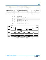
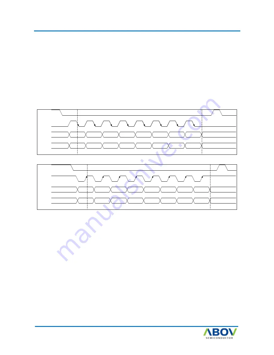
The timing of a SPI transfer where CPHA is one is shown in Figure 10.5 and 10.6.Two wave forms are shown for the SCLK
signal -one for CPOL equals zero and another for CPOL equals one.
Like in the previous cases the falling edge of the nSS lines selects and activates the slave. Compared to the previous
cases, where CPHA equals zero, the transmission is not started and the MSB is not output by the slave at this stage. The
actual transfer is started by a software write to the SP.TDR of the master what causes the clock signal to be generated. The
first edge of the SCLK signal from its inactive to its active state (rising edge if CPOL equals zero and falling edge if CPOL
equals one) causes both the master and the slave to output the MSB of the byte in the SP.TDR.
As shown in Figure 10.3 and 10.4, there is no delay of half a SCLK-cycle. The SCLK line changes its level immediately at
the beginning of the first SCLK-cycle. The data on the input lines is read with the edge of the SCLK line from its active to its
inactive state (falling edge if CPOL equals zero and rising edge if CPOL equals one). After eight clock pulses the
transmission is completed.
D0
D1
D2
D3
D4
D5
D6
D7
D0
D1
D2
D3
D4
D5
D6
D7
MOSI
MISO
SCK
SS
Figure 10.5 SPI Transfer Timing 3/4 (CPHA=1, CPOL=0, MSBF=0)
D0
D1
D2
D3
D4
D5
D6
D7
D0
D1
D2
D3
D4
D5
D6
D7
MOSI
MISO
SCK
SS
Figure 10.6 SPI transfer timing 4/4 (CPHA=1, CPOL=1, MSBF=1)
Summary of Contents for AC30M1x64
Page 3: ...3 246 ABOV Semiconductor INTRODUCTION SECTION 1 INTRODUCTION...
Page 4: ...4 246 4 246 AC30M1x64 1x32 ABOV Semiconductor OVERVIEW CHAPTER 1...
Page 18: ...18 246 18 246 ABOV Semiconductor AC30M1x64 1x32 CPU CHAPTER 2...
Page 22: ...22 246 22 246 ABOV Semiconductor AC30M1x64 1x32 Boot Mode CHAPTER 3...
Page 26: ...26 246 26 246 ABOV Semiconductor AC30M1x64 1x32 SECTION 2 PERIPHERALS...
Page 27: ...27 246 ABOV Semiconductor System Control Unit SCU SYSTEM CONTROL UNIT SCU CHAPTER 1...
Page 69: ...69 246 ABOV Semiconductor Port Control Unit PCU PORT CONTROL UNIT PCU CHAPTER 2...
Page 85: ...85 246 ABOV Semiconductor General Purpose I O GPIO GENERAL PURPOSE I O GPIO CHAPTER 3...
Page 92: ...92 246 92 246 AC30M1x64 1x32 ABOV Semiconductor FLASH MEMORY CONTROLLER CHAPTER 4...
Page 105: ...105 246 ABOV Semiconductor Internal SRAM INTERNAL SRAM CHAPTER 5...
Page 107: ...107 246 ABOV Semiconductor Watch Dog Timer WATCH DOG TIMER WDT CHAPTER 6...
Page 113: ...113 246 ABOV Semiconductor 16 bit Timer 16 BIT TIMER CHAPTER 7...
Page 129: ...129 246 ABOV Semiconductor FRT FREE RUN TIMER FRT CHAPTER 8...
Page 134: ...134 246 134 246 ABOV Semiconductor AC30M1x64 1x32 FUNCTION DESCRIPTION 8 3...
Page 135: ...135 246 UART ABOV Semiconductor UNIVERSAL ASYNCHRONOUS CHAPTER 9 RECEIVER TRANSMITTER UART...
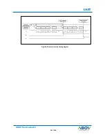
Page 151: ...151 246 ABOV Semiconductor UART Figure 9 6 Transmit interrupt timing diagram...
Page 152: ...152 246 152 246 ABOV Semiconductor AC30M1x64 1x32 SERIAL PERIPHERAL INTERFACE SPI CHAPTER 10...
Page 164: ...164 246 164 246 ABOV Semiconductor AC30M1x64 1x32 I2 C Interface CHAPTER 11...
Page 185: ...185 246 ABOV Semiconductor Motor PWM MOTOR PULSE WIDTH MODULATOR CHAPTER 12 MPWM...
Page 215: ...215 246 ABOV Semiconductor Divider DIVIDER DIV64 CHAPTER 13...
Page 221: ...221 246 ABOV Semiconductor 12 BIT A D Converter 12BIT A D CONVERTER CHAPTER 14...
Page 235: ...235 246 ABOV Semiconductor CHARACTERISTIC SECTION 3 CHARACTERISTIC...
Page 236: ...236 246 236 246 ABOV Semiconductor AC30M1x64 1x32 Electrical Characteristic CHAPTER 1...
Page 243: ...243 246 ABOV Semiconductor Package Package CHAPTER 2...

