178 / 246
178 / 246
ABOV Semiconductor
AC30M1x64/1x32
Acknowledge
11.4.4
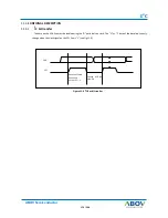
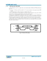
Data transfer with acknowledge is obligatory. The acknowledge-related clock pulse is generated by the master. The
transmitter releases the SDA line (HIGH) during the acknowledge clock pulse.
The receiver must pull down the SDA line during the acknowledge clock pulse so that it remains stable “L” during the “H”
period of this clock pulse (see Figure 11.9). Of course, set-up and hold times must also be taken into account.
When a slave doesn’t acknowledge the slave address (for example, it’s unable to receive or transmit because it’s
performing some real-time function), the data line must be left “H” by the slave. The master can then generate either a
STOP condition to abort the transfer, or a repeated START condition to start a new transfer.
If a slave-receiver does acknowledge the slave address but, sometime later in the transfer cannot receive any more data
bytes, the master must again abort the transfer. This is indicated by the slave generating the not-acknowledge on the first
byte to follow. The slave leaves the data line “H” and the master generates a STOP or a repeated START condition.
If a master-receiver is involved in a transfer, it must signal the end of data to the slave-transmitter by not generating
acknowledge on the last byte that was clocked out of the slave. The slave-transmitter must release the data line to allow
the master to generate a STOP or repeated START condition.
Figure 11.9 I
2
C bus acknowledge
1
2
8
Data Output
By Transmitter
9
ACK
NACK
Clock pulse for ACK
Data Output
By Receiver
SCL from MASTER
Summary of Contents for AC30M1x64
Page 3: ...3 246 ABOV Semiconductor INTRODUCTION SECTION 1 INTRODUCTION...
Page 4: ...4 246 4 246 AC30M1x64 1x32 ABOV Semiconductor OVERVIEW CHAPTER 1...
Page 18: ...18 246 18 246 ABOV Semiconductor AC30M1x64 1x32 CPU CHAPTER 2...
Page 22: ...22 246 22 246 ABOV Semiconductor AC30M1x64 1x32 Boot Mode CHAPTER 3...
Page 26: ...26 246 26 246 ABOV Semiconductor AC30M1x64 1x32 SECTION 2 PERIPHERALS...
Page 27: ...27 246 ABOV Semiconductor System Control Unit SCU SYSTEM CONTROL UNIT SCU CHAPTER 1...
Page 69: ...69 246 ABOV Semiconductor Port Control Unit PCU PORT CONTROL UNIT PCU CHAPTER 2...
Page 85: ...85 246 ABOV Semiconductor General Purpose I O GPIO GENERAL PURPOSE I O GPIO CHAPTER 3...
Page 92: ...92 246 92 246 AC30M1x64 1x32 ABOV Semiconductor FLASH MEMORY CONTROLLER CHAPTER 4...
Page 105: ...105 246 ABOV Semiconductor Internal SRAM INTERNAL SRAM CHAPTER 5...
Page 107: ...107 246 ABOV Semiconductor Watch Dog Timer WATCH DOG TIMER WDT CHAPTER 6...
Page 113: ...113 246 ABOV Semiconductor 16 bit Timer 16 BIT TIMER CHAPTER 7...
Page 129: ...129 246 ABOV Semiconductor FRT FREE RUN TIMER FRT CHAPTER 8...
Page 134: ...134 246 134 246 ABOV Semiconductor AC30M1x64 1x32 FUNCTION DESCRIPTION 8 3...
Page 135: ...135 246 UART ABOV Semiconductor UNIVERSAL ASYNCHRONOUS CHAPTER 9 RECEIVER TRANSMITTER UART...
Page 151: ...151 246 ABOV Semiconductor UART Figure 9 6 Transmit interrupt timing diagram...
Page 152: ...152 246 152 246 ABOV Semiconductor AC30M1x64 1x32 SERIAL PERIPHERAL INTERFACE SPI CHAPTER 10...
Page 164: ...164 246 164 246 ABOV Semiconductor AC30M1x64 1x32 I2 C Interface CHAPTER 11...
Page 185: ...185 246 ABOV Semiconductor Motor PWM MOTOR PULSE WIDTH MODULATOR CHAPTER 12 MPWM...
Page 215: ...215 246 ABOV Semiconductor Divider DIVIDER DIV64 CHAPTER 13...
Page 221: ...221 246 ABOV Semiconductor 12 BIT A D Converter 12BIT A D CONVERTER CHAPTER 14...
Page 235: ...235 246 ABOV Semiconductor CHARACTERISTIC SECTION 3 CHARACTERISTIC...
Page 236: ...236 246 236 246 ABOV Semiconductor AC30M1x64 1x32 Electrical Characteristic CHAPTER 1...
Page 243: ...243 246 ABOV Semiconductor Package Package CHAPTER 2...

