179
/
246
ABOV Semiconductor
I
2
C
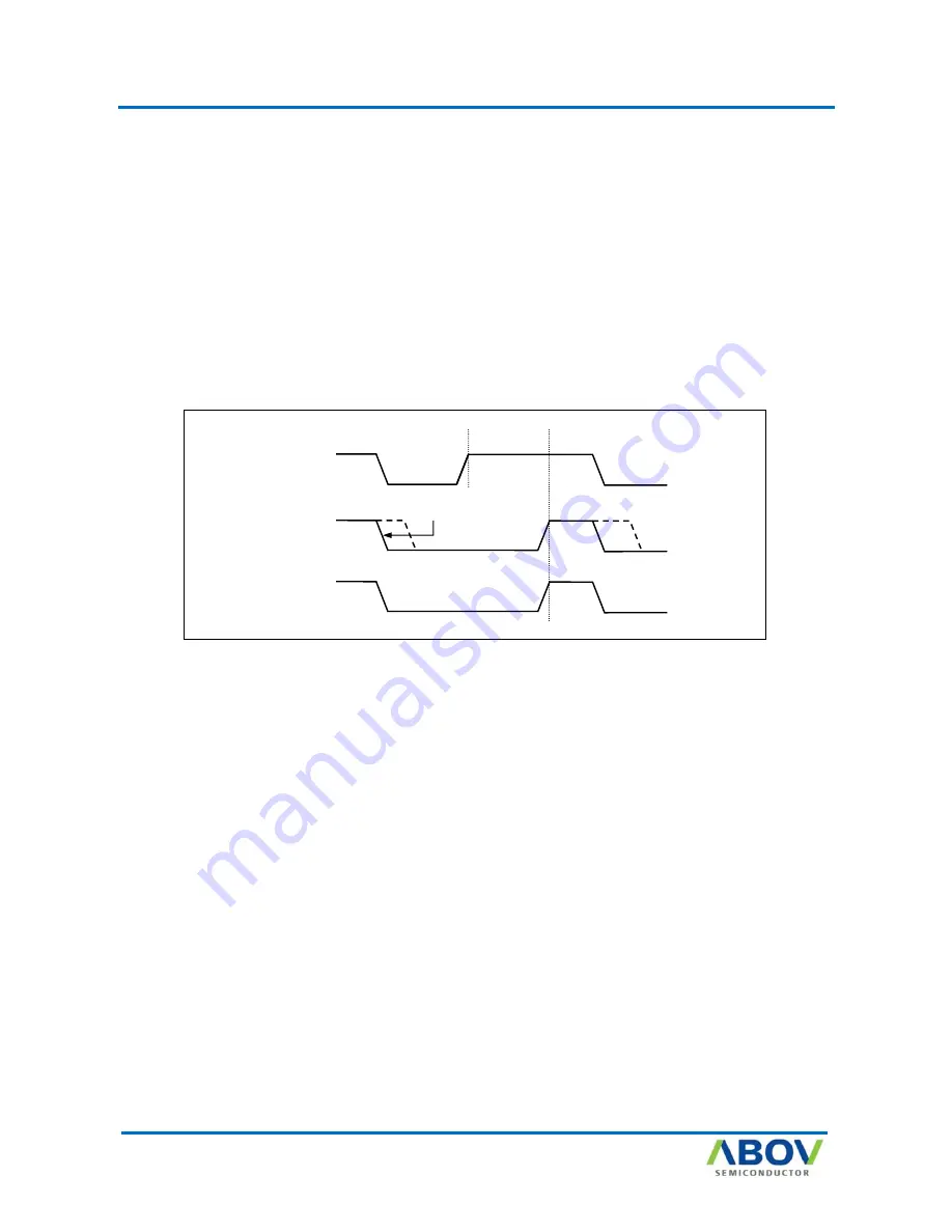
High Counter
Reset
Fast Device
SCLOUT
Slow Device
SCLOUT
SCL
Wait High
Counting
Start High
Counting
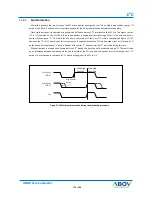
Synchronization
11.4.5
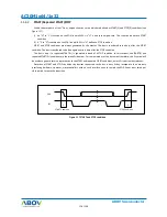
All masters generate their own clock on the SCL line to transfer messages on the I
2
C-bus. Data is only valid during the “H”
period of the clock. A defined clock is therefore needed for the bit-by-bit arbitration procedure to take place.
Clock synchronization is performed using the wired-AND connection of I
2
C interfaces to the SCL line. This means that an
“H” to “L” transition on the SCL line will cause the devices concerned to start counting off their “L” period and, once a
device clock has gone “L”, it will hold the SCL line in that state until the clock “H” state is reached (see Figure 11.10).
However, the “L” to “H” transition of this clock may not change the state of the SCL line if another clock is still within its “L”
by the device with the longest “L” period. Devices with shorter “L” periods enter an “H” wait-state during this time.
When all devices concerned have counted off their “L” period, the clock line will be released and go “H”. There will then
be no difference between the device clocks and the state of the SCL line, and the devices will start counting their “H”
periods. The first device to complete its “H” period will again pull the SCL line “L”.
Figure 11.10 Clock synchronization during the arbitration procedure
Summary of Contents for AC30M1x64
Page 3: ...3 246 ABOV Semiconductor INTRODUCTION SECTION 1 INTRODUCTION...
Page 4: ...4 246 4 246 AC30M1x64 1x32 ABOV Semiconductor OVERVIEW CHAPTER 1...
Page 18: ...18 246 18 246 ABOV Semiconductor AC30M1x64 1x32 CPU CHAPTER 2...
Page 22: ...22 246 22 246 ABOV Semiconductor AC30M1x64 1x32 Boot Mode CHAPTER 3...
Page 26: ...26 246 26 246 ABOV Semiconductor AC30M1x64 1x32 SECTION 2 PERIPHERALS...
Page 27: ...27 246 ABOV Semiconductor System Control Unit SCU SYSTEM CONTROL UNIT SCU CHAPTER 1...
Page 69: ...69 246 ABOV Semiconductor Port Control Unit PCU PORT CONTROL UNIT PCU CHAPTER 2...
Page 85: ...85 246 ABOV Semiconductor General Purpose I O GPIO GENERAL PURPOSE I O GPIO CHAPTER 3...
Page 92: ...92 246 92 246 AC30M1x64 1x32 ABOV Semiconductor FLASH MEMORY CONTROLLER CHAPTER 4...
Page 105: ...105 246 ABOV Semiconductor Internal SRAM INTERNAL SRAM CHAPTER 5...
Page 107: ...107 246 ABOV Semiconductor Watch Dog Timer WATCH DOG TIMER WDT CHAPTER 6...
Page 113: ...113 246 ABOV Semiconductor 16 bit Timer 16 BIT TIMER CHAPTER 7...
Page 129: ...129 246 ABOV Semiconductor FRT FREE RUN TIMER FRT CHAPTER 8...
Page 134: ...134 246 134 246 ABOV Semiconductor AC30M1x64 1x32 FUNCTION DESCRIPTION 8 3...
Page 135: ...135 246 UART ABOV Semiconductor UNIVERSAL ASYNCHRONOUS CHAPTER 9 RECEIVER TRANSMITTER UART...
Page 151: ...151 246 ABOV Semiconductor UART Figure 9 6 Transmit interrupt timing diagram...
Page 152: ...152 246 152 246 ABOV Semiconductor AC30M1x64 1x32 SERIAL PERIPHERAL INTERFACE SPI CHAPTER 10...
Page 164: ...164 246 164 246 ABOV Semiconductor AC30M1x64 1x32 I2 C Interface CHAPTER 11...
Page 185: ...185 246 ABOV Semiconductor Motor PWM MOTOR PULSE WIDTH MODULATOR CHAPTER 12 MPWM...
Page 215: ...215 246 ABOV Semiconductor Divider DIVIDER DIV64 CHAPTER 13...
Page 221: ...221 246 ABOV Semiconductor 12 BIT A D Converter 12BIT A D CONVERTER CHAPTER 14...
Page 235: ...235 246 ABOV Semiconductor CHARACTERISTIC SECTION 3 CHARACTERISTIC...
Page 236: ...236 246 236 246 ABOV Semiconductor AC30M1x64 1x32 Electrical Characteristic CHAPTER 1...
Page 243: ...243 246 ABOV Semiconductor Package Package CHAPTER 2...


