MC80F0304/08/16
November 4, 2011 Ver 2.12
47
counter input 0 (EC0), timer 0 output (T0O), timer 2 output
(T2O) and event counter input 1 (EC1). When the alternate func-
tion is selected by writing “1” in the corresponding bit of PSR0
or PSR1, port pin can be used as a corresponding alternate fea-
tures regardless of the direction register R0IO.
The ADC input channel 1~7 (AN1~AN7), SIO data input (SI),
SIO data output (SOUT) and UART data input (RXD), UART
data output (TXD) and UART clock input (ACLK) can be select-
e d b y s e t t i n g A D C M ( 0 0 E F
H
) , S I O M ( 0 0 E 2
H
) a n d
ASIMR(00E6
H
) register to enable the corresponding peripheral
operation and select operation mode.
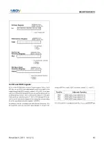
9.2 R1 and R1IO register
R1 is a 5-bit CMOS bidirectional I/O port (address 0C2
H
). Each
I/O pin can independently used as an input or an output through
the R1IO register (address 0C3
H
). When R10 through R17 pins
are used as input ports, an on-chip pull-up resistor can be connect-
ed to them in 1-bit units with a pull-up selection register 1 (PU1).
Each I/O pin of R1 port can be used to open drain output port by
setting the corresponding bit of the open drain selection register
1 (R1OD).
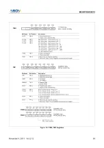
In addition, Port R1 is multiplexed with various alternate func-
tions. The port selection register PSR0 (address 0F8
H
) and PSR1
(address 0F9
H
) control the selection of alternate functions such as
Analog reference voltage input (AVREF), external interrupt 0
(INT0), external interrupt 1 (INT1), PWM 1 output (PWM1O),
PWM 3 output (PWM3O) and buzzer output (BUZO). When the
alternate function is selected by writing “1” in the corresponding
bit of PSR0 or PSR1, port pin can be used as a corresponding al-
ternate features regardless of the direction register R1IO.
The ADC input channel 0 (AN0) and channel 8(AN8) can be se-
lected by setting ADCM(00EF
H
) register to enable ADC and se-
lect channel 0 and channel 8 .
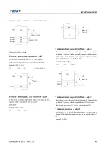
Port Pin
Alternate Function
R00-
R01
R02
R03
R04
R05
R06
R07
INT3 (External interrupt 3)
SCK (SIO clock input/output)
AN1(ADC Input channel 1)
SI (SIO data input)I
AN2 (ADC Input channel 2)
SOUT (SIO data output)
AN3 (ADC Input channel 3)
INT2 (External interrupt 2)
AN4 (ADC Input channel 4)
EC0 (Event counter input 0)
RXD (UART data input)
AN5 (ADC Input channel 5)
T0O (Timer output 0)
TXD (UART data output)
AN6 (ADC Input channel 6)
T2O (Timer output 2)
ACLK (UART clock input)
AN7 (ADC Input channel 7)
EC1 (Event counter input 1)
Port Pin
Alternate Function
R10
R11
R12
R13
R14
R15
R16
R17
AN0 (ADC input channel 0)
AVREF (Analog reference voltage)
PWM1O (PWM 1 output)
INT0 (External Interrupt 0)
PWM3O (PWM 3 output)
INT1 (External Interrupt 1)
BUZO (Buzzer output)
-
-
-
-
AN8


