MC80F0304/08/16
November 4, 2011 Ver 2.12
51
10. CLOCK GENERATOR
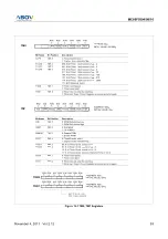
As shown in Figure 10-1 , the clock generator produces the basic
clock pulses which provide the system clock to be supplied to the
CPU and the peripheral hardware. It contains main-frequency
clock oscillator. The system clock operation can be easily ob-
tained by attaching a crystal or a ceramic resonator between the
X
IN
and X
OUT
pin, respectively. The system clock can also be ob-
tained from the external oscillator. In this case, it is necessary to
input a external clock signal to the X
IN
pin and open the X
OUT
pin. There are no requirements on the duty cycle of the external
clock signal, since the input to the internal clocking circuitry is
through a divide-by-two flip-flop, but minimum and maximum
high and low times specified on the data sheet must be observed.
To the peripheral block, the clock among the not-divided original
clock, clocks divided by 1, 2
, 4,...,
up to 4096 can be provided.
Peripheral clock is enabled or disabled by STOP instruction. The
peripheral clock is controlled by clock control register
(CKCTLR). See "11. BASIC INTERVAL TIMER" on page 53
for details.
Figure 10-1 Block Diagram of Clock Generator
10.1
Oscillation Circuit
X
IN
and X
OUT
are the input and output, respectively, a inverting
amplifier which can be set for use as an on-chip oscillator, as
shown in Figure 10-2 .
Figure 10-2 Oscillator Connections
Note:
When using a system clock oscillator, carry out wiring in
the broken line area in Figure 10-2 to prevent any effects from wir-
ing capacities.
- Minimize the wiring length.
- Do not allow wiring to intersect with other signal conductors.
- Do not allow wiring to come near changing high current.
- Set the potential of the grounding position of the oscillator capac-
itor to that of V
SS
. Do not ground to any ground pattern where high
current is present.
- Do not fetch signals from the oscillator.
Internal
PRESCALER
÷
1
Peripheral clock
÷
2
÷
4
÷
8
÷
16
÷
128
÷
256
÷
512
÷
1024
÷
32
÷
64
PS0
PS1
PS2
PS3
PS4
PS5
PS6
PS7
PS8
PS9
PS10
f
EX
(Hz)
PS0
PS3
PS2
PS4
PS1
PS10
PS9
PS5
PS6
PS7
4M
Frequency
period
4M
1M
500K
250K
2M
125K
62.5K
250n
500n
1u
2u
4u
8u
16u
32u
64u
256u
128u
3.906K
7.183K
15.63K
31.25K
PS8
÷
2048
÷
4096
PS12
PS11
1.953K
976
512u
1.024m
Main OSC
SLEEP
f
EX
system clock
PS12
PS11
X
IN
Clock Pulse
Generator
(
÷
2)
Stop
OSC
Circuit
X
OUT
STOP
INOSC
ONP
Circuit
MUX
INOSC
f
XIN
INCLK
Int OSC
Circuit
INOSC
INOSC
(IN4MCLK/IN2MCLK/
7 ~ 3
2 ~ 0
Configuration Option Register (20FF
H
)
IN4MCLKXO/IN2MCLKXO)
Xout
Xin
Vss
C1
C2


