background image

MC80F0304/08/16

56

November 4, 2011   Ver 2.12

time, selecting of output, and clearing of the binary counter.
Clearing the binary counter is repeated within the detection time.

If the malfunction occurs for any cause, the watchdog timer out-
put will become active at the rising overflow from the binary
counters unless the binary counter is cleared. At this time, when
WDTON=1, a reset is generated, which drives the RESET pin to

low to reset the internal hardware. When WDTON=0, a watchdog
timer interrupt (WDTIF) is generated. The WDTON bit is in reg-
ister CLKCTLR.

The watchdog timer temporarily stops counting in the STOP
mode, and when the STOP mode is released, it automatically re-
starts (continues counting).

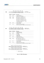
Figure 12-2 WDTR: Watchdog Timer Control Register

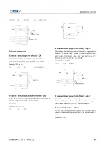
Example: Sets the watchdog timer detection time to 1 sec. at

4.194304MHz 

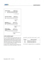
Enable and Disable Watchdog

Watchdog timer is enabled by setting WDTON (bit 4 in
CKCTLR) to “1”. WDTON is initialized to “0” during reset and
it should be set to “1” to operate after reset is released.

Example: Enables watchdog timer for Reset

:

LDM

CKCTLR,#xxx1_xxxxB;

WDTON


 1

:

:

The watchdog timer is disabled by clearing bit 4 (WDTON) of
CKCTLR. The watchdog timer is halted in STOP mode and re-
starts automatically after STOP mode is released.

Watchdog Timer Interrupt

The watchdog timer can be also used as a simple 7-bit timer by
clearing bit4 of CKCTLR to “0”. The interval of watchdog timer
interrupt is decided by Basic Interval Timer. Interval equation is
shown as below.

            T

WDT

 = (WDTR+1) 

×

 Interval of BIT

The stack pointer (SP) should be initialized before using the
watchdog timer output as an interrupt source.

Example: 7-bit timer interrupt set up.

LDM

CKCTLR,#xxx0_xxxxB;

WDTON


0

LDM

WDTR,#8FH

;

WDTCL


1

:

7

6

5

4

3

2

1

0

WDTCL

Clear count flag

0: Free-run count

INITIAL VALUE: 0111 1111

B

ADDRESS: 0F4

H

WDTR

W

W

W

W

1: When the WDTCL is set to “1”, binary counter

is cleared to “0”. And the WDTCL becomes “0” automatically
after one machine cycle. Counter count up again.

7-bit compare data

W

W

W

W

LDM

CKCTLR,#3FH ;

Select 1/1024 clock source

WDTON 

 1, Clear Counter

LDM

WDTR,#08FH

LDM

WDTR,#08FH ;

Clear counter

:

:

:

:

LDM

WDTR,#08FH ;

Clear counter

:

:

:

:

LDM

WDTR,#08FH ;

Clear counter

Within WDT
detection time

Within WDT
detection time

Summary of Contents for MC80F0304

Page 1: ...ABOV SEMICONDUCTOR 8 BIT SINGLE CHIP MICROCONTROLLERS MC80F0304 0308 0316 MC80C0304 0308 0316 User s Manual Ver 2 12...

Page 2: ...or Distributors and Representatives ABOV Semiconductor reserves the right to make changes to any information here in at any time without notice The information diagrams and other data in this manual a...

Page 3: ...ge 80 The format of Instruction Set and Revision History was renewed Fixed some errata VERSION 2 02 SEP 28 2007 This book Fix error in description and diagram of 8 bit event counter VERSION 2 01 MAY 5...

Page 4: ...configuration and Reference ISP Board circuit Add chapters about sequence to enter ISP User mode and ACK mode and update chapters 26 3 to chapter 26 6 Fix some font error in chapter 25 Emulator Board...

Page 5: ...TO DIGITAL CONVERTER 78 15 SERIAL INPUT OUTPUT SIO 81 Transmission Receiving Timing 82 The usage of Serial I O 83 16 UNIVERSAL ASYNCHRONOUS RECEIVER TRANSMITTER UART 85 UART Serial Interface Functions...

Page 6: ...MC80F0304 08 16 6 November 4 2011 Ver 2 12 B MASK ORDER SHEET MC80C0304 x C MASK ORDER SHEET MC80C0308 xi D MASK ORDER SHEET MC80C0316 xii...

Page 7: ...ion time 10 years 512 Bytes On chip Data RAM Included stack memory Minimum Instruction Execution Time 333ns at 12MHz NOP instruction Programmable I O pins LED direct driving can be a source and sink M...

Page 8: ...featured mac ro assembler an in circuit emulator CHOICE Dr TM and OTP programmers There are two different type of programmers such as single type and gang type Macro assembler operates under the MS Wi...

Page 9: ...C80C0308D32 MC80C0308G MC80C0308D 8K bytes 8K bytes 8K bytes 8K bytes 512bytes 32PDIP 32SOP 28SKDIP 28SOP MC80C0304B MC80C0304D32 MC80C0404G MC80C0304D 4K bytes 4K bytes 4K bytes 4K bytes 512bytes 32P...

Page 10: ...uction R0 R1 Buzzer Driver PSW System controller Timing generator System Clock Controller Clock Generator RESET R00 INT3 SCK R01 AN1 SI R02 AN2 SOUT R03 AN3 INT2 R04 AN4 EC0 RXD R05 AN5 T0O TXD R06 AN...

Page 11: ...IP 2 3 4 5 6 7 8 9 10 31 30 29 28 27 26 25 24 23 R12 INT1 BUZO R13 R14 R03 AN3 INT2 R04 AN4 EC0 RXD 1 32 R02 AN2 SOUT R01 AN1 SI R00 INT3 SCK VSS RESET R35 XOUT R34 XIN R33 R05 AN5 T0O TXD R06 AN6 T2O...

Page 12: ...0304 08 16 12 November 4 2011 Ver 2 12 4 PACKAGE DRAWING 1 375 0 015 0 045 TYP 0 100 TYP 0 300 0 300 0 014 0 15 MAX 0 180 MIN 0 020 0 120 28 SKINNY DIP unit inch MAX MIN 1 355 0 021 0 140 0 055 0 008...

Page 13: ...0 25 mm from the lead tip Mold FLASH protrusions or gate burrs shall not exceed 0 15mm per end 7 50 dimension does not include interlead FLASH or protrusion Interlead FLASH or protrusion shall not exc...

Page 14: ...MC80F0304 08 16 14 November 4 2011 Ver 2 12 1 665 0 015 0 045 TYP 0 100 TYP 0 600 0 550 0 012 0 15 MAX 0 190 MIN 0 015 0 120 1 645 0 022 0 140 0 065 0 008 0 530 32 PDIP unit inch MAX MIN...

Page 15: ...MC80F0304 08 16 November 4 2011 Ver 2 12 15 7 45 10 20 21 30 2 55 0 35 TYP 1 27 0 20 MIN 0 8 0 55 32 SOP 10 60 7 55 21 20 2 35 0 45 0 95 unit milimeter MAX MIN TYP 0 40...

Page 16: ...R3 serves the functions of the serial interface following special features in Table 5 4 Port pin Alternate function R00 R01 R02 R03 R04 R05 R06 R07 INT3 External Interrupt Input Port3 SCK SPI CLK AN1...

Page 17: ...ter UART RX R05 AN5 T0O TXD 2 2 I O Analog Input Port 5 Timer0 Output UART TX R06 AN6 T2O ACLK 3 3 I O Analog Input Port 6 Timer2 Output UART Clock R07 AN7 EC1 4 4 I O Analog Input Port 7 Event Counte...

Page 18: ...AN 15 14 ADEN ADS 3 0 ADCM VDD VSS Pin Data Reg Direction Reg Pull up Tr Pull up Reg MUX VDD Data Bus VDD VSS Open Drain Reg SI SI_EN SIOM Noise Filter RD AN 1 ADEN ADS 3 0 VDD VSS Pin Data Reg Direc...

Page 19: ...ilter RD VDD VSS Pin Data Reg Direction Reg Pull up Tr Pull up Reg MUX VDD Data Bus VDD VSS Open Drain Reg INT1E PSR0 1 MUX PWM3OE PSR0 7 BUZOE PSR1 2 PWM3O BUZO SOUT SI SO_OUT_EN SIOM Noise Filter RD...

Page 20: ...CM AN 0 ADEN ADS 3 0 RD VDD VSS Pin Data Reg Direction Reg Pull up Tr Pull up Reg MUX VDD Data Bus VDD VSS Open Drain Reg MUX PWM1OE PSR0 6 PWM1O ADC Reference AVREFS PSR1 3 ADCM MUX VDD Voltage Input...

Page 21: ...CLOCK fXIN 4 RD VDD VSS Data Reg Direction Reg Pull up Tr Pull up Reg MUX VDD Data Bus VDD VSS Open Drain Reg RD VDD VSS XOUT Data Reg Direction Reg Pull up Tr Pull up Reg MUX VDD Data Bus VDD VSS Op...

Page 22: ...extended periods may affect device reliability 7 2 Recommended Operating Conditions 7 3 A D Converter Characteristics Ta 40 85 C VSS 0V VDD 2 7 5 5V fXIN 8MHz Parameter Symbol Condition Specifications...

Page 23: ...5V 20 12 A Hysteresis VT Hysteresis Input1 VDD 5V 0 5 V PFD Voltage VPFD VDD 2 4 2 9 3 4 V POR Voltage2 VPOR VDD 2 2 2 7 3 2 V POR Start Voltage2 VSTART VDD 1 9 V POR Rising Time2 TPOR VDD 40 ms V VDD...

Page 24: ...resented in this section is a statistical summary of data collected on units from different lots over a period of time Typ ical represents the mean of the distribution while max or min represents mean...

Page 25: ...ation 8 6 4 2 0 MHz fXIN 2 3 4 5 6 VDD V Operating Area fXIN 12MHz 10 ISLEEP VDD 2 0 1 5 1 0 0 5 0 mA IDD 2 3 4 5 6 VDD V SLEEP Mode IRCWDT VDD 20 15 10 5 0 A IDD 2 3 4 5 6 VDD V RC WDT in Stop Mode T...

Page 26: ...3 2 1 0 V VIH2 2 3 4 5 6 VDD V Ta 25 C fXIN 4kHz Ta 25 C 1 XIN RESET Hysteresis input 25 C 85 C 25 C 25 C 85 C 25 C VDD VIH3 4 3 2 1 0 V VIH3 2 3 4 5 6 VDD V fXIN 4kHz Ta 25 C Normal input fXIN 4MHz...

Page 27: ...t from that of the MC80C0304 0308 0316 There may be the difference be tween package types PDIP SOP SKDIP The user should modify the value of R and C components to get the proper frequency in exchangin...

Page 28: ...provided in this section are for design guidance only and are not tested or guaranteed In some graphs or tables the data presented are out side specified operating range e g outside specified VDD rang...

Page 29: ...3 2 7 mA IDD 2 3 4 5 6 VDD V Normal Operation 8 6 4 2 0 MHz fXIN 2 3 4 5 6 VDD V Operating Area fXIN 12MHz 10 ISLEEP VDD 2 0 1 5 1 0 0 5 0 mA IDD 2 3 4 5 6 VDD V SLEEP Mode Ta 25 C fXIN 12MHz ISTOP VD...

Page 30: ...3 2 1 0 V VIH2 2 3 4 5 6 VDD V Ta 25 C fXIN 4kHz Ta 25 C 1 XIN RESET Hysteresis input 25 C 85 C 25 C 25 C 85 C 25 C VDD VIH3 4 3 2 1 0 V VIH3 2 3 4 5 6 VDD V fXIN 4kHz Ta 25 C Normal input fXIN 4MHz...

Page 31: ...guaranteed The user needs to take into account that the internal oscillation of the MC80C0104 or MC80C0204 may show different frequency with sample by sample voltage and temperature The internal osci...

Page 32: ...is accepted However if it is used in ex cess of the stack area permitted by the data memory allocating configuration the user processed data may be lost The stack can be located at any position within...

Page 33: ...addressing mode addressing area is from zero page 00H to 0FFH when this flag is 0 If it is set to 1 addressing area is assigned 100H to 1FFH It is set by SETG instruction and cleared by CLRG Overflow...

Page 34: ...re 8 5 Program Memory Map Page Call PCALL area contains subroutine program to reduce At execution of a CALL TCALL PCALL PCL PCH 01FC SP after execution SP before execution 01FD 01FD 01FE 01FF 01FF Pus...

Page 35: ...ons spaces 2 byte interval 0FFFAH and 0FFFBH for External Interrupt 1 0FFFCH and 0FFFDH for Ex ternal Interrupt 0 etc Any area from 0FF00H to 0FFFFH if it is not going to be used its service location...

Page 36: ...Area Memory 0FFFFH PCALL Area 256 Bytes means that the BRK software interrupt is using same address with TCALL0 NOTE TCALL 15 TCALL 14 TCALL 13 TCALL 12 TCALL 11 TCALL 10 TCALL 9 TCALL 8 TCALL 7 TCALL...

Page 37: ...e accessed by bit ma nipulation instruction Do not use read modify write instruc tion Use byte manipulation instruction for example LDM Example To write at CKCTLR LDM CKCTLR 0AH Divide ratio 32 Stack...

Page 38: ...W 0 0 0 0 0 0 byte bit 00D1 Timer 0 register T0 R 0 0 0 0 0 0 0 0 byte Timer 0 data register TDR0 W 1 1 1 1 1 1 1 1 Timer 0 capture data register CDR0 R 0 0 0 0 0 0 0 0 00D2 Timer 1 mode control regi...

Page 39: ...0 0 0 0 0 0 byte bit 00EE Interrupt edge selection register IEDS R W 0 0 0 0 0 0 0 0 byte bit 00EF A D converter mode control register ADCM R W 0 0 0 0 0 0 0 1 byte bit 00F0 A D converter result high...

Page 40: ...8H R0OD R0 Open Drain Selection Register 0C9H R1OD R1 Open Drain Selection Register 0CAH R2OD R2 Open Drain Selection Register 0CBH R3OD R3 Open Drain Selection Register 0D0H TM0 CAP0 T0CK2 T0CK1 T0CK...

Page 41: ...DS3 ADS2 ADS1 ADS0 ADST ADSF 0F0H ADCRH PSSEL1 PSSEL0 ADC8 ADC Result Reg High 0F1H ADCRL ADC Result Register Low 0F2H BITR1 Basic Interval Timer Data Register CKCTLR1 ADRST RCWDT WDTON BTCL BTS2 BTS1...

Page 42: ...sing abs Absolute addressing sets corresponding memory data to Data i e second byte Operand I of command becomes lower level ad dress and third byte Operand II becomes upper level address With 3 bytes...

Page 43: ...command plus the data of X register And it assigns the memory in Direct page ADC AND CMP EOR LDA LDY OR SBC STA STY XMA ASL DEC INC LSR ROL ROR Example G 0 X 0F5H C645 LDA 45H X Y indexed direct page...

Page 44: ...age ADC AND CMP EOR LDA OR SBC STA Example G 0 X 10H 1625 ADC 25H X Y indexed indirect dp Y Processes memory data as Data assigned by the data dp 1 dp of 16 bit pair memory paired by Operand in Direct...

Page 45: ...MC80F0304 08 16 November 4 2011 Ver 2 12 45 1F25E0 JMP 0C025H 25 0E025H jump to E0 0FA00H E7 0E026H 25 0E725H NEXT 1F PROGRAM MEMORY address 0E30AH...

Page 46: ...ter 0 PU0 Each I O pin of R0 port can be used to open drain output port by setting the corresponding bit of the open drain selection register 0 R0OD Figure 9 2 R0 Port Register In addition Port R0 is...

Page 47: ...ate func tions The port selection register PSR0 address 0F8H and PSR1 address 0F9H control the selection of alternate functions such as Analog reference voltage input AVREF external interrupt 0 INT0 e...

Page 48: ...00H R17 R16 R15 R14 R13 R12 R11 R10 Port Direction R1 Direction Register R1IO ADDRESS 0C3H RESET VALUE 00H 0 Input 1 Output Input Output data R1 Pull up PU1 ADDRESS 0FDH RESET VALUE 00H Selection Regi...

Page 49: ...ion Port R3 is multiplexed with alternate functions R30 R31 and R32 can be used as ADC input channel 13 14 and 15 by setting ADCM to enable ADC and select channel 13 14 and 15 R33 R34 and R35 is multi...

Page 50: ...R3 Direction Register R3IO ADDRESS 0C7H RESET VALUE 00H 0 Input 1 Output Input Output data Input data R3 Pull up PU3 ADDRESS 0FDH RESET VALUE 00H Selection Register 0 Disable 1 Enable Pull up Resiste...

Page 51: ...ure 10 1 Block Diagram of Clock Generator 10 1 Oscillation Circuit XIN and XOUT are the input and output respectively a inverting amplifier which can be set for use as an on chip oscillator as shown i...

Page 52: ...XT and capacitor CEXT values and the operating temperature The user needs to take into account variation due to tolerance of external R and C components used Figure 10 1 shows how the RC combination i...

Page 53: ...fter one machine cycle by hardware If the STOP instruction executed after writing 1 to bit RCWDT of CKCTLR it goes into the internal RC oscillated watchdog tim er mode In this mode all of the block is...

Page 54: ...ce clock select 000 fXIN 8 001 fXIN 16 010 fXIN 32 011 fXIN 64 100 fXIN 128 101 fXIN 256 110 fXIN 512 111 fXIN 1024 Clear bit 0 Normal operation free run 1 Clear 8 bit counter BITR to 0 This bit becom...

Page 55: ...imer after the bit WDTON set to 1 maximum error of timer is depend on prescaler ratio of Basic Interval Timer The 7 bit binary counter is cleared by setting WDTCL bit7 of WDTR and the WDTCL is cleared...

Page 56: ...et is released Example Enables watchdog timer for Reset LDM CKCTLR xxx1_xxxxB WDTON 1 The watchdog timer is disabled by clearing bit 4 WDTON of CKCTLR The watchdog timer is halted in STOP mode and re...

Page 57: ...is generated which drives the RESET pin low to reset the internal hardware The main clock oscillator also turns on when a watchdog timer re set is generated in sub clock mode 2 3 n Source clock Binary...

Page 58: ...has six operating modes 8 bit timer counter 16 bit timer counter 8 bit capture 16 bit cap ture 8 bit compare output and 10 bit PWM which are se lected by bit in Timer mode register TM0 and TM1 as sho...

Page 59: ...L 5 4 3 2 1 0 T0CN INITIAL VALUE 00 0000B ADDRESS 0D0H TM0 T0ST T0CK0 T0CK1 CAP0 T0CK2 Bit Name Bit Position Description CAP0 TM0 5 0 Timer Counter mode 1 Capture mode selection flag T0CK2 T0CK1 T0CK0...

Page 60: ...CL 5 4 3 2 1 0 T2CN INITIAL VALUE 00 0000B ADDRESS 0D6H TM2 T2ST T2CK0 T2CK1 CAP2 T2CK2 Bit Name Bit Position Description CAP2 TM2 5 0 Timer Counter mode 1 Capture mode selection flag T2CK2 T2CK1 T2CK...

Page 61: ...ernal clock in put The internal clock has a prescaler divide ratio option of 1 2 4 8 16 32 64 128 256 512 1024 2048 or external clock se lected by control bits TxCK0 TxCK1 TxCK2 of register TMx Figure...

Page 62: ...MER 3 INTERRUPT 1 4 16 TDR2 8 bit TDR3 8 bit T3 8 bit T2 8 bit Comparator Comparator TIMER 2 TIMER 3 BTCL 7 6 5 4 3 2 1 0 T2CN INITIAL VALUE 000000B ADDRESS 0D6H TM2 T2ST T2CK0 T2CK1 CAP2 T2CK2 X X X...

Page 63: ...gister TM2 or 1 4 16 selected by control bits T3CK 1 0 of register TM3 In the Timer 0 timer register T0 in creases from 00H until it matches TDR0 and then reset to 00H The match output of Timer 0 gene...

Page 64: ...event counter function the bit 4 5 of the Port Se lection Register PSR0 address 0F8H is required to be set to 1 After reset the value of timer data register TDRn is initialized to 0 The interval peri...

Page 65: ...from 0000H until it matches TDR2 TDR3 and then resets to 0000H The match output generates Timer 2 interrupt The clock source of the Timer 2 is selected either internal or ex ternal clock by bit T2CK...

Page 66: ...A T1 T0 16 bit Not Timer 1 interrupt EDGE BTCL 7 6 5 4 3 2 1 0 T0CN INITIAL VALUE 00 0000B ADDRESS 0D0H TM0 T0ST T0CK0 T0CK1 CAP0 T0CK2 X X X X X means don t care INITIAL VALUE 00H ADDRESS 0D2H TM1 X...

Page 67: ...TM2 bit CAP3 of timer mode register TM3 for Timer 3 as shown in Figure 13 12 The Timer Counter register is increased in response internal or external input This counting function is same with normal...

Page 68: ...edge transition at external input INTx pin causes the current value in the Timer x register T0 T1 T2 T3 to be captured into registers CDRx CDR0 CDR1 CDR2 CDR3 respectively Af ter captured Timer x reg...

Page 69: ...K 1 0 11 00 01 1 2 8 32 128 512 2048 011 100 101 110 10 INT0 PIN INT1IF 0 Stop 1 Clear and start T1ST INT1 INTERRUPT T1CN CDR1 8 bit T1 8 bit 01 10 11 Capture IEDS 3 2 INT1 PIN BTCL 7 6 5 4 3 2 1 0 T0...

Page 70: ...K 1 0 11 00 01 1 4 16 16 64 256 1024 011 100 101 110 10 INT2 PIN INT3IF 0 Stop 1 Clear and start T3ST INT3 INTERRUPT T3CN CDR3 8 bit T3 8 bit 01 10 11 Capture IEDS 7 6 INT3 PIN BTCL 7 6 5 4 3 2 1 0 T2...

Page 71: ...INT0 Pin Interrupt Request T0 TIME u p c o u n t 0 1 2 3 4 5 6 7 8 9 n n 1 Capture Timer Stop Clear Start Interrupt Interval Period Delay INT0IF Ext INT0 Pin Interrupt Request INT0IF This value is loa...

Page 72: ...bit mode the bits T3CK1 T3CK0 CAP3 and 16BIT of TM3 should be set to 1 re spectively as shown in Figure 13 16 Figure 13 15 16 bit Capture Mode of Timer 0 1 0 Stop 1 Clear and start T0ST T0CN Capture C...

Page 73: ..._0001B INT0 set LDM TM0 0010_1111B CaptureMode LDM TM1 0100_1100B 16bit Mode LDM TDR0 0FFH LDM TDR1 0FFH LDM IEDS 01H Falling Edge SET1 T0E EI 0 Stop 1 Clear and start T2ST T2CN Capture CDR3 CDR2 High...

Page 74: ...PWM1 3 Duty PWM3HR 1 0 T1 3 PDR X Source Clock The relation of frequency and resolution is in inverse proportion Table 13 3 shows the relation of PWM frequency vs resolution If it needed more higher f...

Page 75: ...ADDRESS 0D5H T1PWHR X The value 0 or 1 corresponding your operation BTCL 7 6 5 4 3 2 1 0 T1PWHR1 T1PWHR0 T1PWHR2 T1PWHR3 X X X X W W W W INITIAL VALUE 0FFH ADDRESS 0D3H T1PPR BTCL 7 6 5 4 3 2 1 0 W W...

Page 76: ...DDRESS 0DBH T3PWHR X The value 0 or 1 corresponding your operation BTCL 7 6 5 4 3 2 1 0 T3PWHR1 T3PWHR0 T3PWHR2 T3PWHR3 X X X X W W W W INITIAL VALUE 0FFH ADDRESS 0D9H T3PPR BTCL 7 6 5 4 3 2 1 0 W W W...

Page 77: ...0CH T1PPR FFH T1PDR 7FH T1CK 1 0 00 XIN T1PWHR3 T1PWHR2 T1PWHR1 T1PWHR0 T1PPR 8 bit T1PDR 8 bit Period Duty 1 1 FFH 0 0 7FH 00 clock PWM1E T1ST T1CN 00 3FF Source T1 PWM1O POL 1 Duty Cycle Period Cyc...

Page 78: ...flag ADCIF is set See Figure 14 1 for operation flow The block diagram of the A D module is shown in Figure 14 3 The A D status bit ADSF is set automatically when A D conver sion is completed cleared...

Page 79: ...es resistor string between the AVREF pin and the VSS pin and there will be a large analog sup ply voltage error Figure 14 3 A D Block Diagram AN0 AVREF Sample Hold AN1 AN14 Successive Approximation AD...

Page 80: ...t flow 1 Enable A D converter INITIAL VALUE Undefined ADDRESS 0F1H ADCRL A D Conversion Low Data R W R W BTCL 7 6 5 4 3 2 1 0 PSSEL1 ADCRH ADC8 PSSEL0 INITIAL VALUE 010 B ADDRESS 0F0H A D Conversion H...

Page 81: ...as illustrated in Figure 15 1 The SO pin is de signed to input and output So the Serial I O SIO can be operated with minimum two pin Pin R00 SCK R01 SI and R02 SO pins are controlled by the Serial Mo...

Page 82: ...SIOSF is set to 1 automatically BTCL 7 6 5 4 3 2 1 0 IOSW POL SIOST Serial transmission Clock selection INITIAL VALUE 0000 0001B ADDRESS 0E2H SIOM Serial Input Pin Selection bit 0 SI Pin Selection 1...

Page 83: ...ng mode 2 In case of sending mode write data to be send to SIOR D1 D2 D3 D4 D6 D7 D0 D5 D1 D2 D3 D4 D6 D7 D0 D5 SIOST SCK R00 POL 0 SO R02 SI R01 SIOIF SIO Int Req IOSW 0 D1 D2 D3 D4 D6 D7 D0 D5 IOSWI...

Page 84: ...ecked by reading SIOST and SIOSF As shown in example code wait un til SIOST is changed to 0 and then wait the SIOSF is changed to 1 for completion check Note When external clock is used the frequency...

Page 85: ...baud rate can also be de fined by dividing clocks input to the ACLK pin The UART driver consists of RXR TXR ASIMR ASISR and BRGCR register Universal asynchronous serial I O mode UART can be selected b...

Page 86: ...be written The RESET input sets RXR to 00H Receive shift register This register converts serial data input via the RXD pin to paral leled data When one byte of data is received at this register can n...

Page 87: ...0 Odd parity 11 Even parity UART Tx Rx Enable bit R W 0 Receive Completion Interrupt Control When Error occurs 1 Receive completion interrupt request is not issued when an error occur No parity detect...

Page 88: ...SR OVE R R R 0 No Frame error 1 Framing errorNote1 stop bit not detected UART Parity Error Flag PE UART Overrun Error Flag 0 No overrun error 1 Overrun errorNote2 0 No parity error 1 Parity error Tran...

Page 89: ...errupt request INT_RX occurs Even if an error has occurred the receive data in which the error occurred is still transferred to RXR When ASIMR bit 1 ISRM is cleared to 0 upon occurrence of an error an...

Page 90: ...baud rate generated from the main D0 D1 TxD TX D2 RxD D4 D3 D6 D5 D7 Parity INTERRUPT Stop 1 data frame character bits 1 data frame consists of following bits Start bit 1 bit Character bits 8 bits Par...

Page 91: ...600 52H 0 00 50H 1 73 4AH 0 16 3AH 0 16 2AH 0 16 19200 42H 0 00 40H 1 73 3AH 0 16 2AH 0 16 1AH 0 16 31250 36H 0 53 34H 0 00 30H 0 00 20H 0 00 10H 0 00 38400 32H 0 00 30H 1 73 2AH 0 16 1AH 0 16 57600 2...

Page 92: ...s shown below fBUZ Buzzer frequency fXIN Oscillator frequency Divide Ratio Prescaler divide ratio by BUCK 1 0 BUR Lower 6 bit value of BUZR Buzzer period value The frequency of output signal is contro...

Page 93: ...3 125 2 841 2 604 2 404 2 232 2 083 1 953 28 29 2A 2B 2C 2D 2E 2F 6 098 5 952 5 814 5 682 5 556 5 435 5 319 5 208 3 049 2 976 2 907 2 841 2 778 2 717 2 660 2 604 1 524 1 488 1 453 1 420 1 389 1 359 1...

Page 94: ...Interrupt is generated by BITIF which is set by an overflow in the timer register The AD converter Interrupt is generated by ADCIF which is set by finishing the analog to digital conversion The Watchd...

Page 95: ...Flag Register Reset Interrupt Symbol Priority Hardware Reset External Interrupt 0 External Interrupt 1 External Interrupt 2 External Interrupt 3 UART Rx Interrupt UART Tx Interrupt Serial Input Output...

Page 96: ...ushed onto the stack area The stack pointer decreases 3 times 3 The entry address of the interrupt service program is read from the vector table address and the entry address is loaded to the program...

Page 97: ...ag should be added Example Clearing Interrupt Request Flag Saving Restoring General purpose Register During interrupt acceptance processing the program counter and the program status word are automati...

Page 98: ...3 Multi Interrupt If two requests of different priority levels are received simulta neously the request of higher priority level is serviced If re quests of the interrupt are received at the same time...

Page 99: ...A RETI 18 4 External Interrupt The external interrupt on INT0 INT1 INT2 and INT3 pins are edge triggered depending on the edge selection register IEDS ad dress 0EEH as shown in Figure 18 7 The edge de...

Page 100: ...the next machine cycle If a request is active and conditions are right for it to be acknowledged a hardware subroutine call to the requested service routine will be the next instruction to be ex ecut...

Page 101: ...SS 0F8H PSR0 EC0E INT0E INT2E INT3E 0 R12 1 INT1 0 R03 1 INT2 0 R00 1 INT3 0 R11 1 PWM3O 0 R07 1 EC1 0 R04 1 EC0 LSB MSB BTCL W W W W W W W W IED2H IED3L IED3H IED0H INITIAL VALUE 00H ADDRESS 0EEH IED...

Page 102: ...M Interrupts allow both on chip RAM and Control registers to retain their values If I flag 1 the normal interrupt response takes place If I flag 0 the chip will resume execution starting with the inst...

Page 103: ...perating mode Note The Stop mode is activated by execution of STOP instruc tion after setting the SSCR to 5AH This register should be writ ten by byte operation If this register is set by bit manipula...

Page 104: ...flag 1 the normal interrupt response takes place If I flag 0 the chip will resume execution starting with the instruction fol lowing the STOP instruction It will not vector to interrupt service routi...

Page 105: ...utine Next INSTRUCTION 0 Master Interrupt Enable Bit PSW 2 Corresponding Interrupt Enable Bit IENH IENL Before executing Stop instruction Basic Interval Timer must be set Oscillator XIN pin n 0 BIT Co...

Page 106: ...oth on chip RAM and Control registers to retain their values If I flag 1 the normal interrupt response takes place In this case if the bit WDTON of CKCTLR is set to 0 and the bit WDTE of IENH is set t...

Page 107: ...off output drivers that are sourcing or sinking current if it is prac STOP mode Normal Operation Oscillator XIN pin N 1 N N 2 00 01 FE FF 00 00 N 1 N 2 Clear Basic Interval Timer STOP Instruction Exe...

Page 108: ...ent flow through port doesn t exist First consider the port setting to input mode Be sure that there is no current flow after considering its relationship with external circuit In input mode the pin i...

Page 109: ...12 109 High or Low is decided by considering its relationship with exter nal circuit For example if there is external pull up resistor then it is set to output mode i e to High and if there is externa...

Page 110: ...mplished by holding the RESET pin low for at least 8 oscillator periods within the operating voltage range and oscillation stable it is applied and the internal state is initial ized After reset 65 5m...

Page 111: ...l noise which could not be returned to normal operation and would become malfunc tion state If the CPU tries to fetch the instruction from ineffective code area or RAM area the address fail reset is o...

Page 112: ...ot experiment with it Therefore after final devel opment of user program this function may be experimented or evaluated Figure 21 1 Power Fail Voltage Detector Register Figure 21 2 Example S W of Rese...

Page 113: ...2011 Ver 2 12 113 Figure 21 3 Power Fail Processor Situations at 4MHz operation Internal RESET Internal RESET Internal RESET VDD VDD VDD VPFDMAX VPFDMIN VPFDMAX VPFDMIN VPFDMAX VPFDMIN 65 5mS 65 5mS t...

Page 114: ...k when the high frequency noise is continuing Change system clock to the internal oscillation clock when the XIN XOUT is shorted or opened the main oscillation is stopped except by stop instruction an...

Page 115: ...nal clock source when the external clock is recovered to normal state IN4 2 MCLK CLKXO XO Option The IN4MCLK XO IN2MCLK XO bit of the Device Configuration Area MASK option for MC80F0304 0308 0316 enab...

Page 116: ...confuguration 000 IN4MCLK Internal 4MHz Oscillation R33 R34 Enable 001 IN2MCLK Internal 2MHz Oscillation R33 R34 Enable CLK2 ONP OFP LOCK POR R35EN CLK1 CLK0 010 EXRC External R RC Oscillation R34 En...

Page 117: ...Noise Protector ONP Operation En Disable Bit No ONP Disable OFP Yes Enables Oscillation Fail Processor ONP clock changer Change the Inter clock when oscillation failed No Disables Oscillation Fail Pro...

Page 118: ...MC80F0304 08 16 118 November 4 2011 Ver 2 12 25 EMULATOR EVA BOARD SETTING...

Page 119: ...onnected internally in the Emulator Some circumstance user may connect this circuit ON Output XOUT signal OFF Disconnect circuit SW3 1 This switch select Eva B D Power supply source Normally MDS This...

Page 120: ...MC80F0304 08 16 120 November 4 2011 Ver 2 12 SW6 1 Eva select switch Must be OFF position ON For the MC80F0224 MC80F0448 OFF For the MC80F0316 DIP S W Description ON OFF Setting ON...

Page 121: ...d and the COM1 serial port of your PC 2 Configure the COM1 serial port of your PC as follow ing 3 Turn your target B D power switch ON Your target B D must be configured to enter the ISP mode 4 Run th...

Page 122: ...ation The checksum will be displayed on the checksum box Verify Assures that data in the device matches data in the memory buffer If your device is secured a verification error is detected Lock Secure...

Page 123: ...ESET VPP RST VPP Tx Data1 Rx Data1 ACLK4 VDD 5V ISP Board VSS User target reset circuitry ISP_VPP RST VPP 47K 3 optional 1 If other signals affect UART communiction in ISP mode disconnect these pins b...

Page 124: ...k This mode is only used when failed to de tect user system clock automatically Note Need to connect the ACK pin to ISP B D 26 6 Reference ISP Circuit Diagram and ABOV Supplied ISP Board The ISP softw...

Page 125: ...VDD must be from 4 5 to 5 5V and ISP function is not supported under 2MHz system clock If the user supplied VDD is out of range the external power is needed instead of the target system VDD VDD 5V VSS...

Page 126: ...MC80F0304 08 16 126 November 4 2011 Ver 2 12...

Page 127: ...MC80F0304 08 16 November 4 2011 Ver 2 12 i APPENDIX...

Page 128: ...er that Register auto increment bit Bit Position A bit Bit Position of Accumulator dp bit Bit Position of Direct Page Memory M bit Bit Position of Memory Data 000H 0FFFH rel Relative Addressing Data u...

Page 129: ...N A 111 EI LDM dp imm STA dp STA dp X STA abs TAX STY dp TCALL 14 STC M bit STX dp STX dp Y XAX STOP LOW HIGH 10000 10 10001 11 10010 12 10011 13 10100 14 10101 15 10110 16 10111 17 11000 18 11001 19...

Page 130: ...8 ASL dp 09 2 4 19 ASL dp X 19 2 5 20 ASL abs 18 3 5 21 CMP imm 44 2 2 Compare accumulator contents with memory contents A M N ZC 22 CMP dp 45 2 3 23 CMP dp X 46 2 4 24 CMP abs 47 3 4 25 CMP abs Y 55...

Page 131: ...2 4 67 OR abs 67 3 4 68 OR abs Y 75 3 5 69 OR dp X 76 2 6 70 OR dp Y 77 2 6 71 OR X 74 1 3 72 ROL A 28 1 2 Rotate left through carry N ZC 73 ROL dp 29 2 4 74 ROL dp X 39 2 5 75 ROL abs 38 3 5 76 ROR A...

Page 132: ...STA X F4 1 4 26 STA X FB 1 4 X register auto increment M A X X 1 27 STX dp EC 2 4 Store X register contents in memory M X 28 STX dp Y ED 2 5 29 STX abs FC 3 5 30 STY dp E9 2 4 Store Y register conten...

Page 133: ...dp 0C 2 4 Bit test A with memory Z A M N M7 V M6 MM Z 4 BIT abs 1C 3 5 5 CLR1 dp bit y1 2 4 Clear bit M bit 0 6 CLRA1 A bit 2B 2 2 Clear A bit A bit 0 7 CLRC 20 1 2 Clear C flag C 0 0 8 CLRG 40 1 2 C...

Page 134: ...10 2 2 4 Branch if minus if N 0 then pc pc rel 11 BRA rel 2F 2 4 Branch always pc pc rel 12 BVC rel 30 2 2 4 Branch if overflow bit clear if V 0 then pc pc rel 13 BVS rel B0 2 2 4 Branch if overflow...

Page 135: ...1 4 NOP FF 1 2 No operation 5 POP A 0D 1 4 sp sp 1 A M sp sp sp 1 X M sp sp sp 1 Y M sp sp sp 1 PSW M sp 6 POP X 2D 1 4 7 POP Y 4D 1 4 8 POP PSW 6D 1 4 restored 9 PUSH A 0E 1 4 M sp A sp sp 1 M sp X s...

Page 136: ...s Yes No Yes R35 Use If POR is No No R35 Use ROM Size 4K 8K 16K ONP Use Yes No If ONP is Yes No Yes OFP Use CLK Use Crystal EXRC EXRCXO If ONP is No CLK Use 3 Marking Specification Please check mark i...

Page 137: ...s Yes No Yes R35 Use If POR is No No R35 Use ROM Size 4K 8K 16K ONP Use Yes No If ONP is Yes No Yes OFP Use CLK Use Crystal EXRC EXRCXO If ONP is No CLK Use 3 Marking Specification Please check mark i...

Page 138: ...s Yes No Yes R35 Use If POR is No No R35 Use ROM Size 4K 8K 16K ONP Use Yes No If ONP is Yes No Yes OFP Use CLK Use Crystal EXRC EXRCXO If ONP is No CLK Use 3 Marking Specification Please check mark i...

Reviews: