MC95FG0128A
Aug 02, 2018 Ver.2.9
165
13.4 RESET Noise Canceller
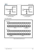
The Figure 13.2 is the Noise canceller diagram for Noise cancel of RESET. It has the Noise cancel
value of about 7us (@V
DD
=5V) to the low input of System Reset.
Figure 13.2 Reset noise canceller time diagram
13.5 Power ON RESET
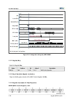
When rising device power, the POR (Power ON Reset) have a function to reset the device. If using
POR, it executes the device RESET function instead of the RESET IC or the RESET circuits.
Figure 13.3 Fast VDD rising time
VDD
nPOR
(Internal Signal)
Internal RESETb
Oscillation
BIT Starts
BIT Overflows
Fast VDD Rise Time
t > T
RNC
t > T
RNC
t > T
RNC
t < T
RNC
t < T
RNC
A
A
’
Summary of Contents for MC95FG0128A
Page 26: ...MC95FG0128A 26 Aug 02 2018 Ver 2 9 4 Package Diagram Figure 4 1 100 pin LQFP package...
Page 27: ...MC95FG0128A Aug 02 2018 Ver 2 9 27 Figure 4 2 80 pin LQFP package...
Page 28: ...MC95FG0128A 28 Aug 02 2018 Ver 2 9 Figure 4 3 80 pin MQFP package...
Page 29: ...MC95FG0128A Aug 02 2018 Ver 2 9 29 Figure 4 4 64 pin LQFP package...
Page 30: ...MC95FG0128A 30 Aug 02 2018 Ver 2 9 Figure 4 5 64 pin LQFP14 package...

