MC95FG0128A
92
Aug 02, 2018 Ver.2.9
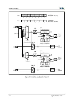
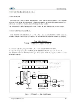
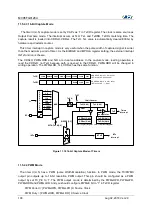
11.5.1.5 16 Bit Capture Mode
The 16-bit capture mode is the same operation as 8-bit capture mode, except that the timer register
uses 16 bits.
The clock source is selected from T0CK[2:0] and T1CK[1:0] must set 11b and 16BIT2 bit must set to
‘1’. The 16-bit mode setting is shown as Figure 11.13.
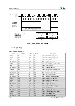
Figure 11.13 16-bit Capture Mode of Timer 0, 1
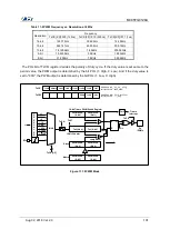
11.5.1.6 PWM Mode
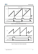
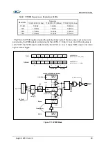
The timer 1 has a PWM (pulse Width Modulation) function. In PWM mode, the T1/PWM1 output pin
outputs up to 10-bit resolution PWM output. This pin should be configured as a PWM output by set
T1
_PE to ‘1’. The period of the PWM output is determined by the T1PPR (PWM period register) +
T1PWHR[3:2] + T1PWHR[1:0]
PWM Period = [ T1PWHR[3:2]T1PPR ] X Source Clock
PWM Duty = [ T1PWHR[1:0] T1PDR ] X Source Clock
Note> T1PPR must be set to higher than T1PDR for guaranteeing operation.
÷
4096
÷
1024
÷
256
P
r
e
s
c
a
l
e
r
MUX
÷
2
÷
4
÷
16
÷
64
EC0
fx
INT0IF
INT0
Interrupt
16-bit Counter
16-bit Data Register
T0CN
Clear
[B6
H
:B3
H
]
T0ST
T0CK[2:0]
3
INT0
EIEDGE.0
T1(8Bit) MSB
T0(8Bit) LSB
CDR1(8Bit)
+CDR0(8BIT)
T1DR(8Bit)
+T0DR(8Bit)
[B6
H
:B3
H
]
[B5
H
:B3
H
]
POL1
16BIT PWM1E
CAP1
T1CK1 T1CK0
T1CN
T1ST
T0EN
T0PE
CAP0
T0CK2 T0CK1 T0CK0
T0CN
T0ST
T1CR
T0CR
1
X
1
X
X
X
X
X
X
1
0
1
1
1
X
X
ADDRESS : B2
H
INITIAL VALUE : 0000_0000
B
ADDRESS : B4
H
INITIAL VALUE : 0000_0000
B
T0IF
Comparator
Clear
Timer0
Interrupt
Summary of Contents for MC95FG0128A
Page 26: ...MC95FG0128A 26 Aug 02 2018 Ver 2 9 4 Package Diagram Figure 4 1 100 pin LQFP package...
Page 27: ...MC95FG0128A Aug 02 2018 Ver 2 9 27 Figure 4 2 80 pin LQFP package...
Page 28: ...MC95FG0128A 28 Aug 02 2018 Ver 2 9 Figure 4 3 80 pin MQFP package...
Page 29: ...MC95FG0128A Aug 02 2018 Ver 2 9 29 Figure 4 4 64 pin LQFP package...
Page 30: ...MC95FG0128A 30 Aug 02 2018 Ver 2 9 Figure 4 5 64 pin LQFP14 package...


