MC95FG0128A
74
Aug 02, 2018 Ver.2.9
11. Peripheral Hardware
11.1 Clock Generator
11.1.1 Overview
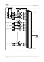
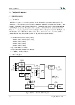
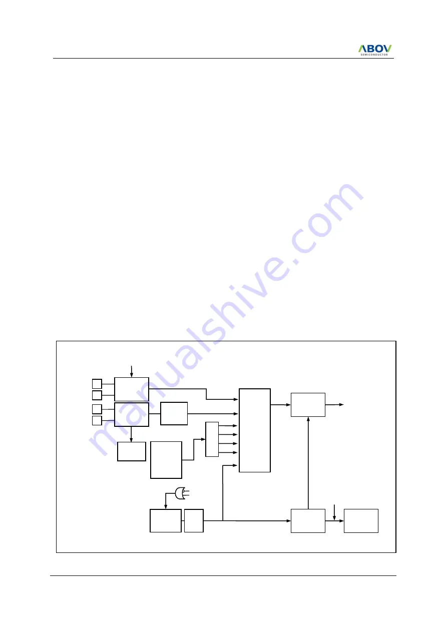
As shown in Figure 11.1, the clock generator produces the basic clock pulses which provide the
system clock to be supplied to the CPU and the peripheral hardware. It contains main-frequency clock
oscillator. The system clock operation can be easily obtained by attaching a crystal between the XIN
and XOUT pin, respectively. The system clock can also be obtained from the external oscillator. In
this case, it is necessary to put the external clock signal into the XIN pin and open the XOUT pin. The
default system clock is INT-RC Oscillator and the default division rate is one. In order to stabilize
system internally, use 1MHz RING oscillator for BIT, WDT and ports de-bounce.
- Calibrated Internal RC Oscillator (8 MHz)
. INT-RC OSC/1 (Default system clock)
. INT-RC OSC/2 (4 MHz)
. INT-RC OSC/4 (2 MHz)
. INT-RC OSC/8 (1 MHz)
- Crystal Oscillator (1~10 MHz)
- Sub-Clock Crystal Oscillator (32.768 KHz)
- PLL output (1.38~20.185 MHz)
11.1.2 Block Diagram
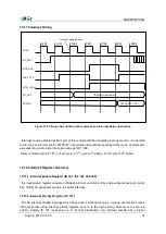
Figure 11.1 Clock Generator Block Diagram
Main
OSC
X
IN
X
OUT
PDOWN
SUB
OSC
SUB
XIN
SUB
XOUT
WT
System
ClockGen.
WDT
BIT
DCLK
System Clock
Masking Control
BIT
Overflow
SCLK
(Core, System,
Peripherals)
Clock
Change
f
XIN
f
SUB
/ f
PLL
f
INTRC
1/2
1/4
1/8
1/1
PLL
(20MHz)
DIV/8
RING-OSC
(1MHz)
PDOWN
STOP1
INT-RC
OSC
(8MHz)
f
RING
DIV
Summary of Contents for MC95FG0128A
Page 26: ...MC95FG0128A 26 Aug 02 2018 Ver 2 9 4 Package Diagram Figure 4 1 100 pin LQFP package...
Page 27: ...MC95FG0128A Aug 02 2018 Ver 2 9 27 Figure 4 2 80 pin LQFP package...
Page 28: ...MC95FG0128A 28 Aug 02 2018 Ver 2 9 Figure 4 3 80 pin MQFP package...
Page 29: ...MC95FG0128A Aug 02 2018 Ver 2 9 29 Figure 4 4 64 pin LQFP package...
Page 30: ...MC95FG0128A 30 Aug 02 2018 Ver 2 9 Figure 4 5 64 pin LQFP14 package...


