MC96F6432
72
June 22, 2018 Ver. 2.9
9. I/O Ports
9.1 I/O Ports
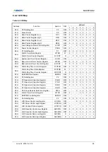
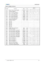
The MC96F6432 has ten groups of I/O ports (P0 ~ P5). Each port can be easily configured by software as I/O
pin, internal pull up and open-drain pin to meet various system configurations and design requirements. Also P0
includes function that can generate interrupt according to change of state of the pin.
9.2 Port Register
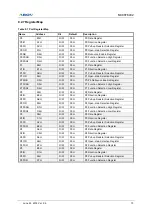
9.2.1 Data Register (Px)
Data Register is a bidirectional I/O port. If ports are configured as output ports, data can be written to the
corresponding bit of the Px. If ports are configured as input ports, the data can be read from the corresponding bit
of the Px.
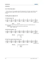
9.2.2 Direction Register (PxIO)
Each I/O pin can be independently used as an input or an output through the PxIO register. Bits cleared in this
register will make the corresponding pin of Px to input mode. Set bits of this register will make the pin to output
mode. Almost bits are cleared by a system reset, but some bits are set by a system reset.
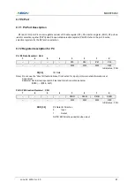
9.2.3 Pull-up Resistor Selection Register (PxPU)
The on-chip pull-up resistor can be connected to I/O ports individually with a pull-up resistor selection register
(PxPU). The pull-up register selection controls the pull-up resister enable/disable of each port. When the
corresponding bit is 1, the pull-up resister of the pin is enabled. When 0, the pull-up resister is disabled. All bits
are cleared by a system reset.
9.2.4 Open-drain Selection Register (PxOD)
There are internally open-drain selection registers (PxOD) for P0 ~ P4 and a bit for P5. The open-drain selection
register controls the open-drain enable/disable of each port. Almost ports become push-pull by a system reset,
but some ports become open-drain by a system reset.
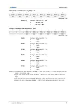
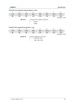
9.2.5 Debounce Enable Register (PxDB)
P0[7:2], P1[2:1], P1[7:6], P52 and P54 support debounce function. Debounce clocks of each ports are fx/1, fx/4,
and fx/4096.
9.2.6 Port Function Selection Register (PxFSR)
These registers define alternative functions of ports. Please remember that these registers should be set
properly for alternative port function. A reset clears the PxFSR register to
‘00H’, which makes all pins to normal
I/O ports.
Summary of Contents for MC96F6432 Series
Page 24: ...MC96F6432 24 June 22 2018 Ver 2 9 4 Package Diagram Figure 4 1 48 Pin LQFP 0707 Package...
Page 25: ...MC96F6432 June 22 2018 Ver 2 9 25 Figure 4 2 44 Pin MQFP Package...
Page 26: ...MC96F6432 26 June 22 2018 Ver 2 9 Figure 4 3 32 Pin LQFP Package...
Page 27: ...MC96F6432 June 22 2018 Ver 2 9 27 Figure 4 4 32 Pin SOP Package...
Page 28: ...MC96F6432 28 June 22 2018 Ver 2 9 Figure 4 5 28 Pin SOP Package...

