MC96F6432
June 22, 2018 Ver. 2.9
29
5. Pin Description
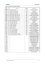
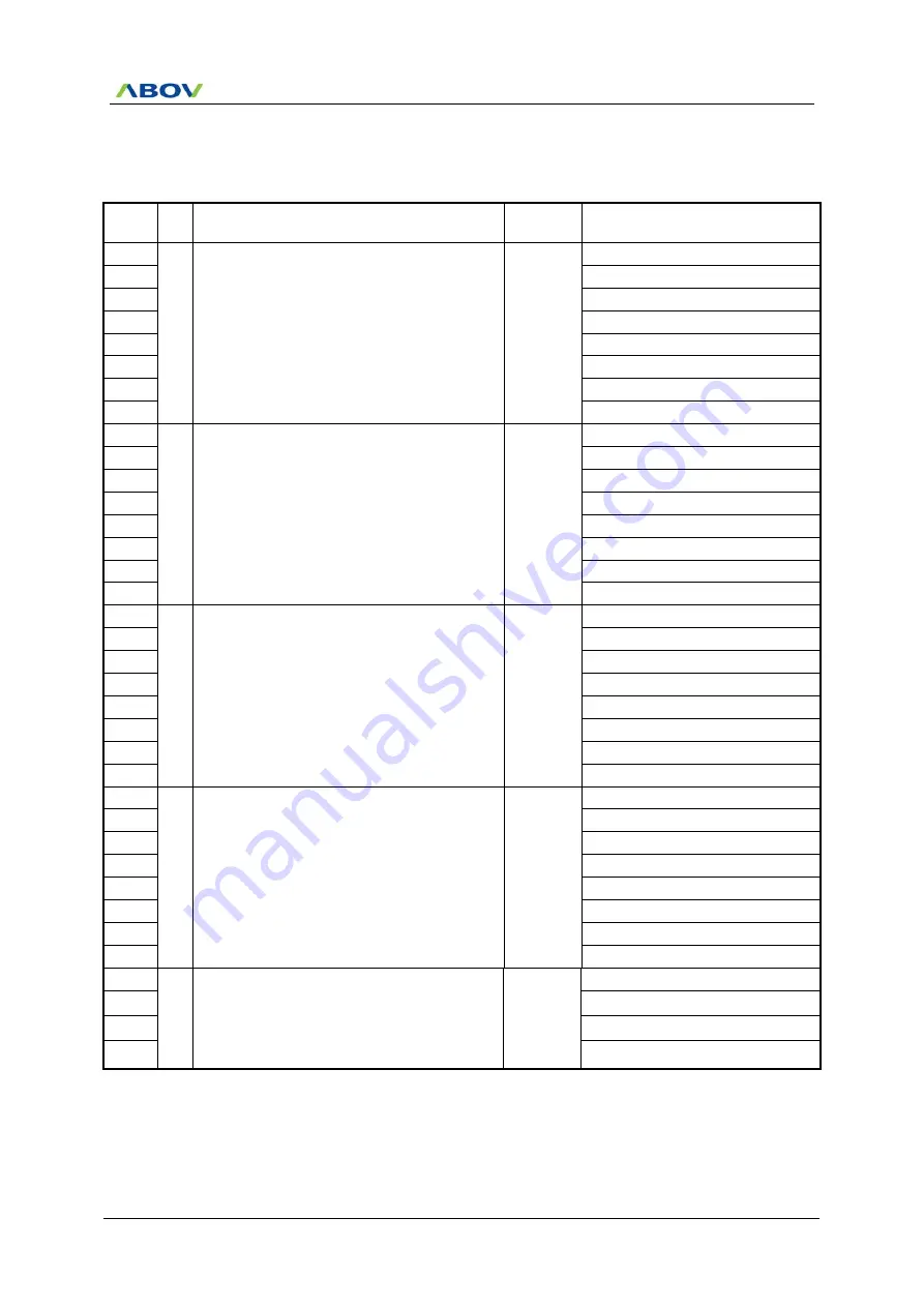
Table 5-1 Normal Pin Description
PIN
Name
I/O
Function
@RESET
Shared with
P00
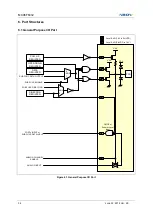
I/O Port 0 is a bit-programmable I/O port which can
be configured as a schmitt-trigger input, a
push-pull output, or an open-drain output.
A pull-up resistor can be specified in 1-bit unit.
Input
EC3/DSDA
P01
T3O/DSCL
P02
AN0/AVREF/EINT0/T4O/PWM4AA
P03
SEG26/AN1/EINT1/PWM4AB
P04
SEG25/AN2/EINT2/PWM4BA
P05
SEG24/AN3/EINT3/PWM4BB
P06
SEG23/AN4/EINT4/PWM4CA
P07
SEG22/AN5/EINT5/PWM4CB
P10
I/O Port 1 is a bit-programmable I/O port which can
be configured as a schmitt-trigger input, a
push-pull output, or an open-drain output.
A pull-up resistor can be specified in 1-bit unit.
The P14
– P17 are not in the 32-pin package.
The P13
– P17 are not in the 28-pin package.
Input
SEG14/AN13/RXD1/SCL1/MISO1
P11
SEG15/AN12/EINT12/T2O/PWM2O
P12
SEG16/AN11/EINT11/T1O/PWM1O
P13
SEG17/AN10/EC1/BUZO
P14
SEG18/AN9/MOSI2
P15
SEG19/AN8/MISO2
P16
SEG20/AN7/EINT7/SCK2
P17
SEG21/AN6/EINT6/SS2
P20
I/O Port 2 is a bit-programmable I/O port which can
be configured as an input, a push-pull output,
or an open-drain output.
A pull-up resistor can be specified in 1-bit unit.
The P23
– P25 are not in the 32-pin package.
The P22
– P27 are not in the 28-pin package.
Input
SEG13/AN14/TXD1/SDA1/MOSI1
P21
SEG12/AN15/SCK1
P22
SEG11/SS1
P23
SEG10
P24
SEG9
P25
SEG8
P26
SEG7
P27
SEG6
P30
I/O Port 3 is a bit-programmable I/O port which can
be configured as an input, a push-pull output.
A pull-up resistor can be specified in 1-bit unit.
The P34
– P37 are only in the 44-pin package.
Input
COM7/SEG5
P31
COM6/SEG4
P32
COM5/SEG3
P33
COM4/SEG2
P34
COM3/SEG1
P35
COM2/SEG0
P36
COM1
P37
COM0
P40
I/O Port 4 is a bit-programmable I/O port which can
be configured as an input, a push-pull output,
or an open-drain output.
A pull-up resistor can be specified in 1-bit unit.
The P43 is only in the 44-pin package.
Input
VLC3/RXD0/SCL0/MISO0
P41
VLC2/TXD0/SDA0/MOSI0
P42
VLC1/SCK0
P43
VLC0/SS0
Summary of Contents for MC96F6432 Series
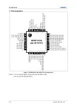
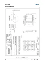
Page 24: ...MC96F6432 24 June 22 2018 Ver 2 9 4 Package Diagram Figure 4 1 48 Pin LQFP 0707 Package...
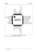
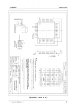
Page 25: ...MC96F6432 June 22 2018 Ver 2 9 25 Figure 4 2 44 Pin MQFP Package...
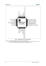
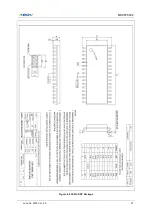
Page 26: ...MC96F6432 26 June 22 2018 Ver 2 9 Figure 4 3 32 Pin LQFP Package...
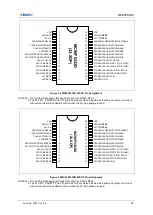
Page 27: ...MC96F6432 June 22 2018 Ver 2 9 27 Figure 4 4 32 Pin SOP Package...
Page 28: ...MC96F6432 28 June 22 2018 Ver 2 9 Figure 4 5 28 Pin SOP Package...


