background image

MC96FM204/FM214 


46 


April 7, 2016 Ver. 1.8 
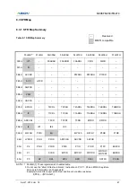
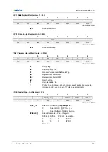
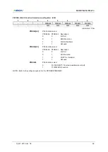


Bit Addressable

7FH

General Purpose

Register

30H

80 Bytes

2FH

20H

16 Bytes
(128bits)

Register Bank 3

(8 Bytes)

1FH

18H

8 Bytes

Register Bank 2

(8 Bytes)

17H

10H

8 Bytes

Register Bank 1

(8 Bytes)

0FH

08H

8 Bytes

Register Bank 0

(8 Bytes)

07H

00H

8 Bytes

R7

R6

R5

R4

R3

R2

R1

R0

7F 7E 7D 7C 7B 7A 79 78

77 76 75 74 73 72 71 70

6F 6E 6D 6C 6B 6A 69 68

67 66 65 64 63 62 61 60

5F 5E 5D 5C 5B 5A 59 58

57 56 55 54 53 52 51 50

4F 4E 4D 4C 4B 4A 49 48

47 46 45 44 43 42 41 40

3F 3E 3D 3C 3B 3A 39 38

37 36 35 34 33 32 31 30

2F 2E 2D 2C 2B 2A 29 28

27 26 25 24 23 22 21 20

1F 1E 1D 1C 1B 1A 19 18

17 16 15 14 13 12 11 10

0F 0E 0D 0C 0B 0A 09 08

07 06 05 04 03 02 01 00


Figure 8.3 Lower 128 Bytes RAM 


Summary of Contents for MC96FM204

Page 1: ...MC96FM204 FM214 April 7 2016 Ver 1 8 1 ABOV SEMICONDUCTOR Co Ltd 8 BIT MICROCONTROLLERS MC96FM204 FM214 User s Manual Ver 1 8 ...

Page 2: ...ption VERSION 1 6 December 5 2012 Modified P13IO and P15IO function descriptions VERSION 1 7 April 14 2015 Add a note at P0 P1 P2 EIFLAG register description and SFR map Change Figure 10 6 and 10 8 in Interrupt Add contents of Flash Protection for Invalid Erase Write VERSION 1 8 April 7 2016 This book Add a note in 7 3 A D Converter Characteristics Add Flash Data Retention Time in Chapter 7 15 Int...

Page 3: ...Frequency Internal RC Oscillator Characteristics 29 7 9 Low Frequency Internal RC Oscillator Characteristics 29 7 10 Internal Watch dog Timer RC Oscillator Characteristics 29 7 11 DC Characteristics 30 7 12 AC Characteristics 31 7 13 SPI Characteristics 32 7 14 Data Retention Voltage in Stop Mode 33 7 15 Internal Flash Rom Characteristics 34 7 16 Input Output Capacitance 34 7 17 Main Clock Oscilla...

Page 4: ... 11 7 Buzzer Driver 112 11 8 SPI 114 11 9 8 Bit A D Converter 120 11 10 Analog Comparator 125 11 11 Operational Amplifier 127 12 Power Down Operation 129 12 1 Overview 129 12 2 Peripheral Operation in IDLE STOP Mode 129 12 3 IDLE Mode 130 12 4 STOP Mode 131 12 5 Release Operation of STOP Mode 132 13 RESET 134 13 1 Overview 134 13 2 Reset Source 134 13 3 RESET Block Diagram 134 13 4 RESET Noise Can...

Page 5: ...e 7 11 RUN IDD1 XIN 8MHz Current 39 Figure 7 12 RUN IDD1 HFIRC 8MHz Current 39 Figure 7 13 RUN IDD1 LFIRC 250kHz Current 40 Figure 7 14 IDLE IDD2 XIN 8MHz Current 40 Figure 7 15 IDLE IDD2 HFIRC 8MHz Current 41 Figure 7 16 IDLE IDD2 LFIRC 250kHz Current 41 Figure 7 17 STOP IDD5 XIN 8MHz Current 42 Figure 8 1 Program Memory 44 Figure 8 2 Data Memory Map 45 Figure 8 3 Lower 128 Bytes RAM 46 Figure 10...

Page 6: ... 0 116 Figure 11 27 SPI Transmit Receive Timing Diagram at CPHA 1 116 Figure 11 28 8 bit ADC Block Diagram 121 Figure 11 29 8 bit A D Converter Timing Chart 121 Figure 11 30 A D Converter Operation Flow 122 Figure 11 31 Analog Comparator Block Diagram 125 Figure 11 32 Operational Amplifier 127 Figure 12 1 IDLE Mode Release Timing by External Interrupt 130 Figure 12 2 STOP Mode Release Timing by Ex...

Page 7: ...ristics 30 Table 7 12 AC Characteristics 31 Table 7 13 SPI Characteristics 32 Table 7 14 Data Retention Voltage in Stop ModeR 33 Table 7 15 Internal flash Rom Characteristics 34 Table 7 16 Input Output Capacitance 34 Table 7 17 Main Clock Oscillator Characteristics 35 Table 7 18 Main Oscillation Stabilization Characteristics 36 Table 8 1 SFR Map Summary 47 Table 8 2 SFR Map 48 Table 9 1 Port Regis...

Page 8: ...1 Peripheral Operation during Power Down Mode 129 Table 12 2 Power Down Operation Register Map 133 Table 13 1 Reset State 134 Table 13 2 Boot Process Description 137 Table 13 3 Reset Operation Register Map 141 Table 15 1 Flash Memory Register Map 152 ...

Page 9: ...al purpose I O basic interval timer watchdog timer 8 16 bit timer counter 16 bit PPG output x 2ch buzzer driving port SPI 8 bit A D converter Analog Comparator Operational Amplifier x 2ch on chip POR LVR LVI on chip oscillator and clock circuitry The Timer2 EINT3 and EINT12 are only in the 20 pin package The EINT2 is in the 20 pin and 16 pin without OP AMP package The MC96FM204 FM214 also supports...

Page 10: ... Reset release level 1 4V Low Voltage Reset 14 level detect 1 60V 2 00V 2 10V 2 20V 2 32V 2 44V 2 59V 2 75V 2 93V 3 14V 3 38V 3 67V 4 00V 4 40V Low Voltage Indicator 13 level detect 2 00V 2 10V 2 20V 2 32V 2 44V 2 59V 2 75V 2 93V 3 14V 3 38V 3 67V 4 00V 4 40V Interrupt Sources External Interrupts EXINT0 3 EINT11 EINT12 6 Timer 0 1 2 3 WDT 1 BIT 1 SPI 1 ADC 1 Comparator 1 Internal RC Oscillator Low...

Page 11: ...ng Information Table 1 1 Ordering Information of MC96FM204 FM214 Device name ROM size IRAM size XRAM size Package MC96FM204D 4k bytes FLASH 256 bytes 20 SOP MC96FM204R 20 TSSOP MC96FM204M 16 SOP MC96FM204H 16 TSSOP MC96FM214M 16 SOP MC96FM214H 16 TSSOP ...

Page 12: ...nd MCU which is attached to user s system The OCD can read or change the value of MCU internal memory and I O peripherals And the OCD also controls MCU internal debugging logic it means OCD controls emulation step run monitoring etc The OCD Debugger program works on Microsoft Windows NT 2000 XP Vista 32bit operating system If you want to see more details please refer to OCD debugger manual You can...

Page 13: ... OCD emulator It can write code in MCU device too because OCD debugging supports ISP In System Programming It does not require additional H W except developer s target system Gang programmer It programs 8 MCU devices at once So it is mainly used in mass production line Gang programmer is standalone type it means it does not require host PC after a program is downloaded from host PC to Gang program...

Page 14: ...EINT11 P01 RESETB SS EC1 P02 XOUT SCK P03 XIN MISO P04 AN0 MOSI OP1IN P05 AN1 OP0OUT Watchdog Timer 6kHz INT RC OSC Basic Interval Timer Power On Reset Low Voltage Reset INT RC OSC 250kHz P2 Port On Chip Debug DSDA DSCL INT RC OSC 8MHz Voltage Down Converter RESETB XIN XOUT CLOCK SYSTEM CONTROL AVSS OP0P P07 P06 AN2 OP0N P07 AN3 OP0P P1 Port P10 AN4 CMP EINT0 P11 AN5 CMP EINT1 P12 AN6 CMPO BUZO P1...

Page 15: ... EINT1 P05 AN1 OP0OUT P04 AN0 MOSI OP1IN P07 AN3 OP0P P06 AN2 OP0N P10 AN4 CMP EINT0 AVSS P16 EC2 P20 DSDA P02 XOUT SCK P01 RESETB SS EC1 P00 T1O PWM1O EINT11 P21 DSCL VDD VSS P03 XIN MISO P15 T2O PWM2O EINT12 P13 AN7 EINT2 P14 EINT3 10 11 Figure 3 1 MC96FM204 20SOP TSSOP Pin Assignment NOTE On On Chip Debugging ISP uses P2 1 0 pin as DSDA DSCL ...

Page 16: ... be selected as a push pull output or an input with pull up resistor by software control when the 16 pin with OP AMP package is used MC96FM214M H 1 2 8 3 4 5 6 7 9 14 13 12 11 10 16 15 P13 AN7 EiNT2 P20 DSDA P02 XOUT SCK P01 RESETB SS EC1 P00 T1O PWM1O EINT11 P21 DSCL VDD P03 XIN MISO P12 AN6 BUZO P05 AN1 P04 AN0 MOSI P07 AN3 P06 AN2 P11 AN5 EINT1 P10 AN4 EINT0 VSS Figure 3 3 MC96FM214 16SOP TSSOP...

Page 17: ...MC96FM204 FM214 April 7 2016 Ver 1 8 17 4 Package Diagram Figure 4 1 20 Pin SOP Package ...

Page 18: ...MC96FM204 FM214 18 April 7 2016 Ver 1 8 Figure 4 2 20 Pin TSSOP Package ...

Page 19: ...MC96FM204 FM214 April 7 2016 Ver 1 8 19 Figure 4 3 16 Pin SOP Package ...

Page 20: ...MC96FM204 FM214 20 April 7 2016 Ver 1 8 Figure 4 4 16 Pin TSSOP Package ...

Page 21: ...P package Input AN4 CMP EINT0 P11 AN5 CMP EINT1 P12 AN6 CMPO BUZO P13 I O Output AN7 EINT2 P14 EINT3 P15 T2O PWM2O EINT12 P16 EC2 P20 I O Port 2 is a bit programmable I O port which can be configured as an input a push pull output or an open drain output A pull up resistor can be specified in 1 bit unit Input DSDA P21 DSCL EINT11 I O External interrupt input Timer 1 capture input Input P00 T1O PWM...

Page 22: ...R M H device Input P06 AN2 OP0OUT I O OP AMP 0 output The OP0OUT is only in MC96FM204D R M H device Input P05 AN1 OP1IN I O OP AMP 1 input The OP1IN is only in MC96FM204D R M H device Input P04 AN0 MOSI RESETB I O System reset pin with a pull up resistor when it is selected as the RESETB by CONFIGURE OPTION 2 Input P01 SS EC1 XIN I O Main oscillator pins Input P03 MISO XOUT P02 SCK AVSS A D conver...

Page 23: ... VDD OPEN DRAIN REGISTER DATA REGISTER DIRECTION REGISTER MUX 0 1 MUX 1 0 CMOS or Schmitt Level Input ANALOG CHANNEL ENABLE ANALOG INPUT PORTx INPUT or SUB FUNC DATA INPUT SUB FUNC DIRECTION SUB FUNC ENABLE SUB FUNC DATA OUTPUT Level Shift ExtVDD to 1 8V Level Shift 1 8V to ExtVDD Figure 6 1 General Purpose I O Port ...

Page 24: ... 1 0 INTERRUPT ENABLE EXTERNAL INTERRUPT Q D CP r VDD FLAG CLEAR POLARITY REG MUX 1 0 DEBOUNCE ENABLE Q D CP r DEBOUNCE CLK CMOS or Schmitt Level Input ANALOG CHANNEL ENABLE ANALOG INPUT PORTx INPUT or SUB FUNC DATA INPUT SUB FUNC DIRECTION SUB FUNC ENABLE SUB FUNC DATA OUTPUT Level Shift ExtVDD to 1 8V Level Shift 1 8V to ExtVDD Figure 6 2 External Interrupt I O Port ...

Page 25: ...Temperature TSTG 65 150 C NOTE Stresses beyond those listed under Absolute Maximum Ratings may cause permanent damage to the device This is a stress rating only and functional operation of the device at any other conditions beyond those indicated in the operational sections of this specification is not implied Exposure to absolute maximum rating conditions for extended periods may affect device re...

Page 26: ...ltage VAN VSS VDD V Analog Ground Voltage AVSS VSS VSS 0 3 A DC Input Leakage Current IAN VDD 5 12V 2 μA Sample Hold Time TSH VDD 5 12V 4 μS A DC Current IADC Enable VDD 5 12V 1 2 mA Disable 0 1 μA NOTES 1 When VDD is lower than 2 7V the ADC resolution is worse 7 4 Power On Reset Characteristics Table 7 4 Power On Reset Characteristics TA 40 C 85 C VDD 1 8V 5 5V VSS 0V Parameter Symbol Conditions ...

Page 27: ...R VLVI The LVR can select all levels but LVI can select other levels except 1 60V 1 60 1 75 V 1 85 2 00 2 15 1 95 2 10 2 25 2 05 2 20 2 35 2 17 2 32 2 47 2 29 2 44 2 59 2 39 2 59 2 79 2 55 2 75 2 95 2 73 2 93 3 13 2 94 3 14 3 34 3 18 3 38 3 58 3 37 3 67 3 97 3 70 4 00 4 30 4 10 4 40 4 70 Hysteresis V 10 100 mV Minimum Pulse Width tLW 100 μS LVR and LVI Current IBL Enable Both VDD 3V 8 0 14 0 μA En...

Page 28: ...1 Characteristics TA 20 C 60 C VDD 1 8V 5 5V VSS 0V Parameter Symbol Conditions MIN TYP MAX Unit Input Offset Voltage VOF VDD 3 0V VIN 1 2VDD 25 mV Common mode Rejection Ratio CMRR VDD 3 0V VIN 1 0V 50 70 dB Power Supply Rejection Ratio PSRR VDD 3 0V VIN 1 0V 40 70 Open Loop Voltage Gain AMP0 VDD 3 0V 80 dB DC Gain Error AMP1 ERR VDD 3 0V 0 03V VIN 0 2V 1 Common mode Input Voltage VIN VDD 3 0V 0 V...

Page 29: ...Disable 0 1 μA 7 9 Low Frequency Internal RC Oscillator Characteristics Table 7 9 Low Frequency Internal RC Oscillator Characteristics TA 40 C 85 C VDD 1 8V 5 5V VSS 0V Parameter Symbol Conditions MIN TYP MAX Unit Frequency fLFIRC 250 kHz Tolerance VDD 2 0V 5 5V TA 20 C to 60 C 1 3 Clock Duty Ratio TOD 40 50 60 Stabilization Time tLFS 100 μS 7 10 Internal Watch dog Timer RC Oscillator Characterist...

Page 30: ...D 5 0V 25 50 100 kΩ VDD 3 0V 50 100 200 RPU2 VI 0V TA 25 C RESETB VDD 5 0V 150 250 400 kΩ VDD 3 0V 300 500 700 OSC feedback resistor RX XIN VDD XOUT VSS TA 25 C VDD 5V 600 1200 2000 kΩ Supply Current IDD1 Run fXIN 8MHz VDD 5V 10 3 0 6 0 mA fHFIRC 8MHz 2 0 4 0 fXIN 8MHz VDD 3V 10 2 0 4 0 mA fLFIRC 250kHz 100 150 μA IDD2 Idle fXIN 8MHz VDD 5V 10 2 0 4 0 mA fHFIRC 8MHz 1 0 2 0 fXIN 8MHz VDD 3V 10 1 0...

Page 31: ...B input low width tRST VDD 5 V 10 μS Interrupt Input High Low width tIWH tIWL All interrupts VDD 5 V 200 nS External Counter Input High Low Pulse Width tECWH tECWL EC0 EC1 VDD 5 V 200 External Counter Transition Time tREC tFEC EC0 EC1 VDD 5 V 20 tIWH tIWL External Interrupt tRST 0 2VDD 0 2VDD 0 8VDD RESETB tECWH tECWL EC0 EC1 0 2VDD 0 8VDD tFEC tREC Figure 7 1 AC Timing ...

Page 32: ...200 Output Clock High Low Pulse Width tSCKH tSCKL Internal SCK source 70 Input Clock High Low Pulse Width External SCK source 70 First Output Clock Delay Time tFOD Internal External SCK source 100 Output Clock Delay Time tDS 50 Input Setup Time tDIS 100 Input Hold Time tDIH 150 SS Output Input SCK CPOL 0 Output Input SCK CPOL 1 Output Input MISO MOSI Data Input tFOD tSCK tSCKL tSCKH 0 8VDD 0 2VDD ...

Page 33: ...Active VDD NOTE tWAIT is the same as the selected bit overflow of BIT X 1 BIT Clock INT Request Execution of STOP Instruction Data Retention Stop Mode Normal Operating Mode 0 8VDD tWAIT VDDDR Figure 7 3 Stop Mode Release Timing when Initiated by an Interrupt NOTE tWAIT is the same as 4096 X 4 X 8 fHFIRC 16 4 mS at fx 1MHz VDD RESETB Execution of STOP Instruction Data Retention Stop Mode Oscillatio...

Page 34: ... Time tFBR 5 μS Flash Programming Frequency fPGM 0 4 MHz Endurance of Write Erase NFWE 100 000 Times Flash Data Retention Time tRT 10 Years NOTE During a flash operation SCLK 1 0 of SCCR must be set to 00 or 01 Main X TAL or HF INT RC or LF INT RC OSC for system clock 7 16 Input Output Capacitance Table 7 16 Input Output Capacitance TA 40 C 85 C VDD 0V Parameter Symbol Condition MIN TYP MAX Unit I...

Page 35: ...rystal Main oscillation frequency 1 8V 5 5V 0 4 4 2 MHz 2 7V 5 5V 0 4 10 0 3 0V 5 5V 0 4 12 0 Ceramic Oscillator Main oscillation frequency 1 8V 5 5V 0 4 4 2 MHz 2 7V 5 5V 0 4 10 0 3 0V 5 5V 0 4 12 0 External Clock XIN input frequency 1 8V 5 5V 0 4 4 2 MHz 2 7V 5 5V 0 4 10 0 3 0V 5 5V 0 4 12 0 XIN XOUT C1 C2 Figure 7 5 Crystal Ceramic Oscillator XIN XOUT External Clock Source Open Figure 7 6 Exter...

Page 36: ...l fx 1MHz Oscillation stabilization occurs when VDD is equal to the minimum oscillator voltage range 60 mS Ceramic 10 mS External Clock fXIN 0 4 to 12MHz XIN input high and low width tXH tXL 42 1250 nS tXH tXL XIN 0 2VDD 0 8VDD 1 fXIN Figure 7 7 Clock Timing Measurement at XIN 7 19 Operating Voltage Range 1 8 0 4MHz 2 7 5 5 12 0MHz fXIN 0 4 to 12MHz Supply voltage V 4 2MHz 10 0MHz 3 0 Figure 7 8 O...

Page 37: ...s 0 1uF capacitor should be within 1cm from the VDD pin of MCU on the PCB layout This 0 01uF capacitor is alternatively for noise immunity X tal The main crystal should be as close by the MCU as possible 0 1uF VDD VCC The MCU power line VDD and VSS should be separated from the high current part at a DC power node on the PCB layout DC Power Figure 7 9 Recommended Circuit and Layout ...

Page 38: ...commended C2 47uF 25V more The R1 and C2 should be as close by the C3 as possible 3 The C3 capacitor is used for temperature compensation because an electrolytic capacitor becomes worse characteristics at low temperature Recommended C3 ceramic capacitor 2 2uF more The C3 should be within 1cm from VDD pin of MCU on the PCB layout 4 The above circuit is recommended to improve noise immunity EFT Surg...

Page 39: ...to operate properly only within the specified range The data presented in this section is a statistical summary of data collected on units from different lots over a period of time Typical represents the mean of the distribution while max or min represents mean 3σ and mean 3σ respectively where σ is standard deviation Figure 7 11 RUN IDD1 XIN 8MHz Current Figure 7 12 RUN IDD1 HFIRC 8MHz Current 0 ...

Page 40: ...8 Figure 7 13 RUN IDD1 LFIRC 250kHz Current Figure 7 14 IDLE IDD2 XIN 8MHz Current 0 00 20 00 40 00 60 00 80 00 100 00 120 00 2 7V 3 0V 3 3V uA 40 25 85 0 00 0 20 0 40 0 60 0 80 1 00 1 20 1 40 1 60 2 7V 3 0V 3 3V 4 5V 5 0V 5 5V mA 40 25 85 ...

Page 41: ...Ver 1 8 41 Figure 7 15 IDLE IDD2 HFIRC 8MHz Current Figure 7 16 IDLE IDD2 LFIRC 250kHz Current 0 56 0 58 0 60 0 62 0 64 0 66 0 68 4 5V 5 0V 5 5V mA 40 25 85 0 00 10 00 20 00 30 00 40 00 50 00 60 00 70 00 2 7V 3 0V 3 3V uA 40 25 85 ...

Page 42: ...MC96FM204 FM214 42 April 7 2016 Ver 1 8 Figure 7 17 STOP IDD5 XIN 8MHz Current 0 00 0 50 1 00 1 50 2 00 2 50 2 7V 3 0V 3 3V 4 5V 5 0V 5 5V uA 40 25 85 ...

Page 43: ...his device has just 4k bytes program memory space Figure 8 1 shows the map of the lower part of the program memory After reset the CPU begins execution from location 0000H Each interrupt is assigned a fixed location in program memory The interrupt causes the CPU to jump to that location where it commences execution of the service routine External interrupt 1 for example is assigned to location 000...

Page 44: ...MC96FM204 FM214 44 April 7 2016 Ver 1 8 FFFFH 0000H 4k Bytes 0FFFH Figure 8 1 Program Memory 4k Bytes Including Interrupt Vector Region ...

Page 45: ...upper 128 bytes and SFR space occupying the same block of addresses 80H through FFH although they are physically separate entities The lower 128 bytes of RAM are present in all 8051 devices as mapped in Figure 8 3 The lowest 32 bytes are grouped into 4 banks of 8 registers Program instructions call out these registers as R0 through R7 Two bits in the Program Status Word select which register bank ...

Page 46: ... Bytes 07H 00H 8 Bytes R7 R6 R5 R4 R3 R2 R1 R0 7F 7E 7D 7C 7B 7A 79 78 77 76 75 74 73 72 71 70 6F 6E 6D 6C 6B 6A 69 68 67 66 65 64 63 62 61 60 5F 5E 5D 5C 5B 5A 59 58 57 56 55 54 53 52 51 50 4F 4E 4D 4C 4B 4A 49 48 47 46 45 44 43 42 41 40 3F 3E 3D 3C 3B 3A 39 38 37 36 35 34 33 32 31 30 2F 2E 2D 2C 2B 2A 29 28 27 26 25 24 23 22 21 20 1F 1E 1D 1C 1B 1A 19 18 17 16 15 14 13 12 11 10 0F 0E 0D 0C 0B 0A...

Page 47: ...L T1BDRH 0B0H ADCCRL T0CR T0CNT T0DR SPICR SPIDR 0A8H IE IE1 IE2 IE3 0A0H EIFLAG P2PU EO EIPOL0 EIPOL1 P0DB P1DB 98H LVRCR P2IO P2OD ADCCRH ADCDR SHTDR 90H P2 P0IO P0OD P0PU P1IO P1OD P1PU BUZCR 88H P1 SCCR BITCR BITCNT WDTCR WDTDR WDTCNT BUZDR 80H P0 SP DPL DPH DPL1 DPH1 RSTFR PCON NOTE 1 00H 8H 1 These registers are bit addressable 2 Do not use the direct bit test and branch instruction on P0 P1...

Page 48: ...l Register WDTCR R W 0 0 0 0 8EH Watch Dog Timer Data Register WDTDR W 1 1 1 1 1 1 1 1 Watch Dog Timer Counter Register WDTCNT R 0 0 0 0 0 0 0 0 8FH BUZZER Data Register BUZDR R W 1 1 1 1 1 1 1 1 90H P2 Data Register P2 R W 0 0 91H P0 Direction Register P0IO R W 0 0 0 0 0 0 0 0 92H P0 Open drain Selection Register P0OD R W 0 0 0 0 0 0 0 0 93H P0 Pull up Resistor Selection Register P0PU R W 0 0 0 0...

Page 49: ... W 0 0 0 ABH Interrupt Enable Register 3 IE3 R W 0 0 ACH Reserved ADH Reserved AEH Reserved AFH Reserved B0H A D Converter Control Low Register ADCCRL R W 0 0 0 0 0 0 0 0 B1H Reserved B2H Timer 0 Control Register T0CR R W 0 0 0 0 0 0 B3H Timer 0 Counter Register T0CNT R 0 0 0 0 0 0 0 0 B4H Timer 0 Data Register T0DR R W 1 1 1 1 1 1 1 1 B5H SPI Control Register SPICR R W 0 0 0 0 0 0 0 0 B6H SPI Dat...

Page 50: ...T2ADRH R W 1 1 1 1 1 1 1 1 C6H Timer 2 B Data Low Register T2BDRL R W 1 1 1 1 1 1 1 1 C7H Timer 2 B Data High Register T2BDRH R W 1 1 1 1 1 1 1 1 C8H Oscillator Control Register OSCCR R W 1 0 0 0 0 C9H Reserved CAH Reserved CBH Reserved CCH Reserved CDH Reserved CEH Reserved CFH Reserved D0H Program Status Word Register PSW R W 0 0 0 0 0 0 0 0 D1H Reserved D2H Reserved D3H Reserved D4H Reserved D5...

Page 51: ...W 0 0 0 0 0 EDH Port 0 Function Selection High Register P0FSRH R W 0 0 0 0 0 0 0 0 EEH Port 1 Function Selection Low Register P1FSR R W 0 0 0 0 0 0 0 0 EFH Reserved F0H B Register B R W 0 0 0 0 0 0 0 0 F1H Reserved F2H Reserved F3H Reserved F4H Reserved F5H Reserved F6H Reserved F7H Reserved F8H Interrupt Priority Register 1 IP1 R W 0 0 0 0 0 0 F9H Reserved FAH Flash Sector Address High Register F...

Page 52: ...R W R W R W R W R W R W R W R W Initial value 00H B B Register SP Stack Pointer 81H 7 6 5 4 3 2 1 0 SP R W R W R W R W R W R W R W R W Initial value 07H SP Stack Pointer DPL Data Pointer Register Low 82H 7 6 5 4 3 2 1 0 DPL R W R W R W R W R W R W R W R W Initial value 00H DPL Data Pointer Low DPH Data Pointer Register High 83H 7 6 5 4 3 2 1 0 DPH R W R W R W R W R W R W R W R W Initial value 00H ...

Page 53: ... 00H CY Carry Flag AC Auxiliary Carry Flag F0 General Purpose User Definable Flag RS1 Register Bank Select bit 1 RS0 Register Bank Select bit 0 OV Overflow Flag F1 User Definable Flag P Parity Flag Set cleared by hardware each instruction cycle to indicate an odd even number of 1 bits in the accumulator EO Extended Operation Register A2H 7 6 5 4 3 2 1 0 TRAP_EN DPSEL2 DPSEL1 DPSEL0 R W R W R W R W...

Page 54: ...Resistor Selection Register PxPU The on chip pull up resistor can be connected to I O ports individually with a pull up resistor selection register PxPU The pull up register selection controls the pull up resister enable disable of each port When the corresponding bit is 1 the pull up resister of the pin is enabled When 0 the pull up resister is disabled All bits are cleared by a system reset 9 2 ...

Page 55: ... R W 00H Port 0 Function Selection High Register P0FSRL ECH R W 00H Port 0 Function Selection Low Register P1 88H R W 78H P1 Data Register P1IO 94H R W 78H P1 Direction Register P1OD 95H R W 78H P1 Open drain Selection Register P1PU 96H R W 00H P1 Pull up Resistor Selection Register P1DB A7H R W 00H P1 Debounce Enable Register P1FSR EEH R W 00H Port 1 Function Selection Register P2 90H R W 00H P2 ...

Page 56: ...nitial value 00H P0 7 0 I O Data Note Do not use the direct bit test and branch instruction for input port more detail information is at Appendix B Example Avoid direct input port bit test and branch condition as below If P00 if P0 0x01 P0IO P0 Direction Register 91H 7 6 5 4 3 2 1 0 P07IO P06IO P05IO P04IO P03IO P02IO P01IO P00IO R W R W R W R W R W R W R W R W Initial value 00H P0IO 7 0 P0 Data I...

Page 57: ...B R W R W R W Initial value 00H DBCLK 1 0 Configure Debounce Clock of Port DBCLK1 DBCLK0 Description 0 0 fx SCLK 0 1 fx 4 1 0 fx 4096 1 1 Reserved P00DB Configure Debounce of P00 Port 0 Disable 1 Enable NOTES 1 If the same level is not detected on enabled pin three or four times in a row at the sampling clock the signal is eliminated as noise 2 A pulse level should be input for the duration of 3 c...

Page 58: ...FSRH07 PFSRH06 Description 0 0 I O Port 0 1 OP0P Function 1 0 AN3 Function 1 1 Not used PFSRH0 5 4 P06 Function select PFSRH05 PFSRH04 Description 0 0 I O Port 0 1 OP0N Function 1 0 AN2 Function 1 1 Not used PFSRH0 3 2 P05 Function select PFSRH03 PFSRH02 Description 0 0 I O Port 0 1 OP0OUT Function 1 0 AN1 Function 1 1 Not used PFSRH0 1 0 P04 Function select PFSRH01 PFSRH00 Description 0 0 I O Por...

Page 59: ...03 Function select PFSRL04 PFSRL03 Description 0 0 I O Port 0 1 MISO Function 1 0 XIN for Oscillator 1 1 Not used PFSRL0 2 1 P02 Function select PFSRL02 PFSRL01 Description 0 0 I O Port 0 1 SCK Function 1 0 XOUT for Oscillator 1 1 Not used PFSRL00 P00 Function select 0 I O Port EINT11 function possible when input 1 T1O PWM1O Function NOTE Refer to the configure option 2 for the P01 RESETB SS EC1 ...

Page 60: ...P12 P11 P10 R W R W R W R W R W R W R W Initial value 78H P1 6 0 I O Data Note Do not use the direct bit test and branch instruction for input port more detail information is at Appendix B Example Avoid direct input port bit test and branch condition as below If P10 if P1 0x01 P1IO P1 Direction Register 94H 7 6 5 4 3 2 1 0 P16IO P15IO P14IO P13IO P12IO P11IO P10IO R W R W R W R W R W R W R W Initi...

Page 61: ...r A7H 7 6 5 4 3 2 1 0 P15DB P14DB P13DB P11DB P10DB R W R W R W R W R W Initial value 00H P15DB Configure Debounce of P15 Port 0 Disable 1 Enable P14DB Configure Debounce of P14 Port 0 Disable 1 Enable P13DB Configure Debounce of P13 Port 0 Disable 1 Enable P11DB Configure Debounce of P11 Port 0 Disable 1 Enable P10DB Configure Debounce of P10 Port 0 Disable 1 Enable NOTES 1 If the same level is n...

Page 62: ...select 0 I O Port EINT3 function possible when input 1 AN7 Function PFSR1 5 4 P12 Function select PFSR15 PFSR14 Description 0 0 I O Port EINT2 function possible when input 0 1 CMPO Function 1 0 AN6 Function 1 1 BUZO Function PFSR1 3 2 P11 Function select PFSR13 PFSR12 Description 0 0 I O Port EINT1 function possible when input 0 1 CMP Function 1 0 AN5 Function 1 1 Not used PFSR1 1 0 P10 Function s...

Page 63: ...h instruction for input port more detail information is at Appendix B Example Avoid direct input port bit test and branch condition as below If P20 if P2 0x01 P2IO P2 Direction Register 99H 7 6 5 4 3 2 1 0 P21IO P20IO R W R W Initial value 00H P2IO 1 0 P2 Data I O Direction 0 Input 1 Output P2PU P2 Pull up Resistor Selection Register A1H 7 6 5 4 3 2 1 0 P21PU P20PU R W R W Initial value 00H P2PU 1...

Page 64: ...d by bit 7 of IE EA When EA is set to 0 all interrupts are disabled when EA is set to 1 interrupts are individually enabled or disabled through the other bits of the interrupt enable registers The EA bit is always cleared to 0 jumping to an interrupt service vector and set to 1 executing the RETI instruction The MC96FM204 FM214 supports a four level priority scheme Each maskable interrupt is indiv...

Page 65: ...larity 1 register EIPOL1 as shown in Figure 10 1 Also each external interrupt source has enable disable bits The External interrupt flag register EIFLAG provides the status of external interrupts EINT0 Pin EIPOL0 1 EINT1 Pin FLAG0 FLAG1 EINT2 Pin EINT3 Pin FLAG2 FLAG3 EINT11 Pin EINT12 Pin FLAG11 FLAG12 INT0 Interrupt INT1 Interrupt INT2 Interrupt INT3 Interrupt INT4 Interrupt INT5 Interrupt Figur...

Page 66: ...T0 EIPOL0 1 EIFLAG 0 EIFLAG 1 EINT1 ADC ADCIFR SPI SPIIFR IE FLAG0 FLAG1 EINT2 EIFLAG 2 EIFLAG 3 EINT3 FLAG2 FLAG3 Timer 1 T1IFR IE2 Timer 2 T0IFR Timer 0 T2IFR BIT BITIFR IE3 WDT WDTIFR EINT11 EIFLAG 4 EIFLAG 5 EINT12 FLAG11 FLAG12 EA Release Stop Sleep Level2 Level0 Level3 Level1 Figure 10 2 Block Diagram of Interrupt NOTES 1 The release signal for stop idle mode may be generated by all interrup...

Page 67: ...Interrupt INT16 IE2 4 17 Maskable 0083H INT17 IE2 5 18 Maskable 008BH INT18 IE3 0 19 Maskable 0093H WDT Interrupt INT19 IE3 1 20 Maskable 009BH BIT Interrupt INT20 IE3 2 21 Maskable 00A3H INT21 IE3 3 22 Maskable 00ABH INT22 IE3 4 23 Maskable 00B3H INT23 IE3 5 24 Maskable 00BBH For maskable interrupt execution EA bit must set 1 and specific interrupt must be enabled by writing 1 to associated bit i...

Page 68: ...Flag 0 1 Program Counter low Byte SP SP 1 M SP PCL 2 Program Counter high Byte SP SP 1 M SP PCH 3 Interrupt Vector Address occurrence Interrupt Vector Address 4 ISR Interrupt Service Routine move execute 5 Return from ISR RETI 6 Program Counter high Byte recovery PCH SP 1 7 Main Program execution 10 Program Counter low Byte recovery PCL SP 1 8 IE EA Flag 1 9 ...

Page 69: ...ng of Interrupt Enable Register Case b Interrupt flag Register Figure 10 5 Effective Timing of Interrupt Flag Register Interrupt Flag Register Command Next Instruction Next Instruction After executing next instruction interrupt flag result is effective Interrupt Enable Register command Next Instruction Next Instruction After executing IE set clear enable register is effective ...

Page 70: ...than INT1 is occurred Then INT0 is served immediately and then the remain part of INT1 service routine is executed If the priority level of INT0 is same or lower than INT1 INT0 will be served after the INT1 service has completed An interrupt service routine may be only interrupted by an interrupt of higher priority and if two interrupts of different priority occur at the same time the higher level...

Page 71: ... Saving Restore Process Diagram and Sample Source Main Task Saving Register Restoring Register Interrupt Service Task INTxx PUSH PSW PUSH DPL PUSH DPH PUSH B PUSH ACC Interrupt_Processing POP ACC POP B POP DPH POP DPL POP PSW RETI 02H 25H 00B3H 00B4H Basic Interval Timer Vector Table Address 0EH 2EH 0125H 0126H Basic Interval Timer Service Routine Address 01H 00B5H Interrupt Latched Interrupt goes...

Page 72: ...12 1 Interrupt Enable Register IE IE1 IE2 IE3 Interrupt enable register consists of global interrupt control bit EA and peripheral interrupt control bits Total 24 peripherals are able to control interrupt 10 12 2 Interrupt Priority Register IP IP1 The 24 interrupts are divided into 6 groups which have each 4 interrupt sources A group can be assigned 4 levels interrupt priority using interrupt prio...

Page 73: ...d The flag is cleared when the interrupt service routine is executed Alternatively the flag can be cleared by writing a 0 to it 10 12 4 External Interrupt Polarity Register EIPOL0 EIPOL1 The external interrupt polarity 0 register EIPOL0 and external interrupt polarity 1 register EIPOL1 determines which type of rising falling both edge interrupt Initially default value is no interrupt at any edge ...

Page 74: ...rrupt Flag Register EIPOL0 A4H R W 00H External Interrupt Polarity 0 Register EIPOL1 A5H R W 00H External Interrupt Polarity 1 Register 10 13 Interrupt Register Description The interrupt register is used for controlling interrupt functions Also it has external interrupt control registers The interrupt register consists of interrupt enable register IE interrupt enable register 1 IE1 interrupt enabl...

Page 75: ...Disable External Interrupt 11 0 Disable 1 Enable INT3E Enable or Disable External Interrupt 3 0 Disable 1 Enable INT2E Enable or Disable External Interrupt 2 0 Disable 1 Enable INT1E Enable or Disable External Interrupt 1 0 Disable 1 Enable INT0E Enable or Disable External Interrupt 0 0 Disable 1 Enable IE1 Interrupt Enable Register 1 A9H 7 6 5 4 3 2 1 0 INT11E INT10E INT9E R W R W R W Initial val...

Page 76: ... Timer 2 Interrupt 0 Disable 1 Enable INT13E Enable or Disable Timer 1 Interrupt 0 Disable 1 Enable INT12E Enable or Disable Timer 0 Interrupt 0 Disable 1 Enable IE3 Interrupt Enable Register 3 ABH 7 6 5 4 3 2 1 0 INT20E INT19E R W R W Initial value 00H INT20E Enable or Disable BIT Interrupt 0 Disable 1 Enable INT19E Enable or Disable WDT Interrupt 0 Disable 1 Enable ...

Page 77: ... IP1 IP0 R W R W R W R W R W R W Initial value 00H IP1 Interrupt Priority Register 1 F8H 7 6 5 4 3 2 1 0 IP15 IP14 IP13 IP12 IP11 IP10 R W R W R W R W R W R W Initial value 00H IP 5 0 IP1 5 0 Select Interrupt Group Priority IP1x IPx Description 0 0 level 0 lowest 0 1 level 1 1 0 level 2 1 1 level 3 highest ...

Page 78: ...tion as below If FLAG0 if EIFLAG 0x01 EIPOL0 External Interrupt Polarity 0 Register A4H 7 6 5 4 3 2 1 0 POL3 POL2 POL1 POL0 R W R W R W R W R W R W R W R W Initial value 00H EIPOL0 7 0 External interrupt EINT0 EINT1 EINT2 EINT3 polarity selection POLn 1 0 Description 0 0 No interrupt at any edge 0 1 Interrupt on rising edge 1 0 Interrupt on falling edge 1 1 Interrupt on both of rising and falling ...

Page 79: ...ht In order to stabilize system internally it is used 1MHz INT RC oscillator on POR Calibrated Internal RC Oscillator 8 MHz 250kHz INT RC OSC 1 8 MHz when fHFIRC 250 kHz when fLFIRC INT RC OSC 2 4 MHz when fHFIRC 125 kHz when fLFIRC INT RC OSC 4 2 MHz when fHFIRC 62 5 kHz when fLFIRC INT RC OSC 8 1 MHz when fHFIRC 31 3 kHz when fLFIRC Default system clock Main Crystal Oscillator 0 4 12 MHz Interna...

Page 80: ...SCLK1 SCLK0 R W R W R W Initial value 00H WONS Control the Operation of WDT RC Oscillation during STOP mode 0 WDTRC Oscillator is disabled at STOP mode 1 WDTRC Oscillator is enabled at STOP mode NOTES 1 When this bit is 1 the WDTRC oscillator 6kHz is oscillated and selected as the clock source of the WDT block in the STOP mode but the WDTRC stops and the BIT overflow clock is the clock source for ...

Page 81: ...nternal RC oscillator post divider selection IRCS1 IRCS0 Description 0 0 fIRC 8 1MHz when fHFIRC 31 3kHz when fLFIRC 0 1 fIRC 4 2MHz when fHFIRC 62 5kHz when fLFIRC 1 0 fIRC 2 4MHz when fHFIRC 125kHz when fLFIRC 1 1 fIRC 1 8MHz when fHFIRC 250kHz when fLFIRC HFIRCE Control the operation of the high frequency internal RC oscillator 0 Enable operation of HF INT RC OSC 1 Disable operation of HF INT R...

Page 82: ...ng It also provides a basic interval timer interrupt BITIFR The MC96FM204 FM214 has these basic interval timer BIT features During Power On BIT gives a stable clock generation time On exiting Stop mode BIT gives a stable clock generation time As timer function timer interrupt occurrence 11 2 2 Block Diagram BIT Clock BCK 2 0 8 Bit Up Counter BITCNT BCLR clear BITIFR To interrupt block selected bit...

Page 83: ... 3 2 1 0 BITCNT7 BITCNT6 BITCNT5 BITCNT4 BITCNT3 BITCNT2 BITCNT1 BITCNT0 R R R R R R R R Initial value 00H BITCNT 7 0 BIT Counter BITCR Basic Interval Timer Control Register 8BH 7 6 5 4 3 2 1 0 BITIFR BCLR BCK2 BCK1 BCK0 R W R W R W R W R W Initial value 01H BITIFR When BIT Interrupt occurs this bit becomes 1 For clearing bit write 0 to this bit or auto clear by INT_ACK signal 0 BIT interrupt no g...

Page 84: ...ts up After 1 machine cycle this bit is cleared to 0 automatically The watchdog timer consists of 8 bit binary counter and the watchdog timer data register When the value of 8 bit binary counter is equal to the 8 bits of WDTCNT the interrupt request flag is generated This can be used as Watchdog timer interrupt or reset of CPU in accordance with the bit WDTRSON The input clock source of watch dog ...

Page 85: ... Map Table 11 3 Watch Dog Timer Register Map Name Address Dir Default Description WDTCNT 8EH R 00H Watch Dog Timer Counter Register WDTDR 8EH W FFH Watch Dog Timer Data Register WDTCR 8DH R W 00H Watch Dog Timer Control Register 11 3 5 Watch Dog Timer Register Description The watch dog timer register consists of watch dog timer counter register WDTCNT watch dog timer data register WDTDR and watch ...

Page 86: ...TDR 7 0 Set a period WDT Interrupt Interval BIT Interrupt Interval x WDTDR Value 1 NOTE Do not write 0 in the WDTDR register WDTCR Watch Dog Timer Control Register 8DH 7 6 5 4 3 2 1 0 WDTEN WDTRSON WDTCL WDTIFR R W R W R W R W Initial value 00H WDTEN Control WDT Operation 0 Disable 1 Enable WDTRSON Control WDT RESET Operation 0 Free Running 8 bit timer 1 Watch Dog Timer RESET ON WDTCL Clear WDT Co...

Page 87: ... have counter and data register The counter register is increased by internal clock input Timer 0 can use the input clock with one of 1 4 16 64 256 1024 and 4096 prescaler division rates T0CK 2 0 When the value of T0CNT and T0DR is identical in timer 0 a match signal is generated and the interrupt of Timer 0 occurs T0CNT value is automatically cleared by match signal It can be also cleared by soft...

Page 88: ...r 1 8 Figure 11 6 8 Bit Timer Counter 0 Example T0CNT Value Timer 0 T0IFR Interrupt TIME 1 2 3 4 5 6 n 2 n 1 n Interrupt Period PCP x n 1 0 Count Pulse Period PCP Up count Match with T0DR Occur Interrupt Occur Interrupt Occur Interrupt ...

Page 89: ...c a l e r fx M U X 3 T0CK 2 0 T0EN 8 bit Counter Comparator 8 bit Data Register T0CNT 8Bit T0DR 8Bit MSB LSB MSB LSB T0IFR INT_ACK Clear fx 1 To interrupt block T0CC Clear Match signal Match fx 4 fx 16 fx 64 fx 256 fx 1024 fx 4096 Figure 11 7 8 Bit Timer 0 Block Diagram ...

Page 90: ...timer counter 0 register consists of timer 0 counter register T0CNT timer 0 data register T0DR and timer 0 control register T0CR 11 4 4 2 Register Description for Timer Counter 0 T0CNT Timer 0 Counter Register B3H 7 6 5 4 3 2 1 0 T0CNT7 T0CNT6 T0CNT5 T0CNT4 T0CNT3 T0CNT2 T0CNT1 T0CNT0 R R R R R R R R Initial value 00H T0CNT 7 0 T0 Counter T0DR Timer 0 Data Register B4H 7 6 5 4 3 2 1 0 T0DR7 T0DR6 ...

Page 91: ...becomes 1 For clearing bit write 0 to this bit or auto clear by INT_ACK signal 0 T0 Interrupt no generation 1 T0 Interrupt generation T0CK 2 0 Select Timer 0 clock source fx is a system clock frequency T0CK2 T0CK1 T0CK0 Description 0 0 0 fx 4096 0 0 1 fx 1024 0 1 0 fx 256 0 1 1 fx 64 1 0 0 fx 16 1 0 1 fx 4 1 1 0 fx 1 1 1 1 Not used T0CC Clear timer 0 Counter 0 No effect 1 Clear the Timer 0 counter...

Page 92: ...Timer 1 outputs PWM wave form through PWM1O port in the PPG mode Table 11 5 Timer 1 Operating Modes T1EN PFSRL00 T1MS 1 0 T1CK 2 0 Timer 1 1 1 00 XXX 16 Bit Timer Counter Mode 1 0 01 XXX 16 Bit Capture Mode 1 1 10 XXX 16 Bit PPG Mode one shot mode 1 1 11 XXX 16 Bit PPG Mode repeat mode 11 5 2 16 Bit Timer Counter Mode The 16 bit timer counter mode is selected by control register as shown in Figure...

Page 93: ...To interrupt block A Match Buffer Register A A Match T1CC Reload Pulse Generator T1O R T1EN 3 T1CK 2 0 2 T1MS1 T1MS0 T1CC 0 0 X T1CK2 T1CRL X ADDRESS BAH INITIAL VALUE 0000_0000B T1CK1 T1CK0 T1IFR T1POL T1ECE T1CNTR X X X X X X T1EN Figure 11 8 16 Bit Timer Counter Mode for Timer 1 Figure 11 9 16 Bit Timer Counter 1 Example T1CNTH L Value Timer 1 T1IFR Interrupt TIME 1 2 3 4 5 6 n 2 n 1 n Interrup...

Page 94: ...RL According to EIPOL1 registers setting the external interrupt EINT11 function is chosen Of course the EINT11 pin must be set as an input port A Match T1CC T1EN P r e s c a l e r fx M U X fx 2 fx 4 fx 64 fx 512 fx 2048 fx 8 fx 1 16 bit Counter T1CNTH T1CNTL 16 bit B Data Register T1BDRH T1BDRL Clear Edge Detector T1ECE EC1 Comparator 16 bit A Data Register T1ADRH T1ADRL T1IFR INT_ACK Clear To int...

Page 95: ...Capture Mode T1CNTH L Interrupt Request FLAG11 XXH Interrupt Interval Period FFFFH 01H FFFFH 01H YYH 01H Ext EINT11 PIN Interrupt Request T1IFR FFFFH FFFFH YYH 00H 00H 00H 00H 00H T1CNTH L Value Interrupt Request FLAG11 TIME 1 2 3 4 5 6 n 2 n 1 n Interrupt Interval Period 0 Count Pulse Period PCP Up count T1BDRH L Load Ext EINT11 PIN ...

Page 96: ... fx 512 fx 2048 fx 8 fx 1 Comparator 16 bit Counter T1CNTH T1CNTL 16 bit B Data Register T1BDRH T1BDRL Clear B Match Edge Detector T1ECE EC1 Buffer Register B Comparator 16 bit A Data Register T1ADRH T1ADRL T1IFR INT_ACK Clear To interrupt block A Match Buffer Register A Reload Pulse Generator T1O PWM1O R T1EN 3 T1CK 2 0 2 T1EN T1CRH 1 ADDRESS BBH INITIAL VALUE 0000_0000B T1MS1 T1MS0 T1CC 1 1 X T1...

Page 97: ...1 T1BDRH L 5 T1ADRH L PWM1O A Match 2 T1BDRH L T1ADRH L PWM1O A Match 3 T1BDRH L 0000H Low Level X 1 2 4 5 6 8 M 1 0 Timer 1 clock Counter T1ADRH L T1 Interrupt PWM1O B Match One shot Mode T1MS 10b and Start High T1POL 0b Set T1EN 0 Clear and Start 3 7 M A Match 1 T1BDRH L 5 T1ADRH L PWM1O A Match 2 T1BDRH L T1ADRH L PWM1O A Match 3 T1BDRH L 0000H Low Level Figure 11 14 16 Bit PPG Mode Timming cha...

Page 98: ...0 2 A Match T1CC T1EN A Match T1CC T1EN Figure 11 15 16 Bit Timer 1 Block Diagram 11 5 6 Register Map Table 11 6 Timer 2 Register Map Name Address Dir Default Description T1ADRH BDH R W FFH Timer 1 A Data High Register T1ADRL BCH R W FFH Timer 1 A Data Low Register T1BDRH BFH R W FFH Timer 1 B Data High Register T1BDRL BEH R W FFH Timer 1 B Data Low Register T1CRH BBH R W 00H Timer 1 Control High ...

Page 99: ...T1ADRL3 T1ADRL2 T1ADRL1 T1ADRL0 R W R W R W R W R W R W R W R W Initial value FFH T1ADRL 7 0 T1 A Data Low Byte NOTE Do not write 0000H in the T1ADRH T1ADRL register when PPG mode T1BDRH Timer 1 B Data High Register BFH 7 6 5 4 3 2 1 0 T1BDRH7 T1BDRH6 T1BDRH5 T1BDRH4 T1BDRH3 T1BDRH2 T1BDRH1 T1BDRH0 R W R W R W R W R W R W R W R W Initial value FFH T1BDRH 7 0 T1 B Data High Byte T1BDRL Timer 1 B Da...

Page 100: ...sable 1 Timer 1 enable Counter clear and start T1MS 1 0 Control Timer 1 Operation Mode T1MS1 T1MS0 Description 0 0 Timer counter mode T1O toggle at A match 0 1 Capture mode The A match interrupt can occur 1 0 PPG one shot mode PWM1O 1 1 PPG repeat mode PWM1O T1CC Clear Timer 1 Counter 0 No effect 1 Clear the Timer 1 counter When write automatically cleared 0 after being cleared counter ...

Page 101: ... External clock EC1 T1IFR When T1 Interrupt occurs this bit becomes 1 For clearing bit write 0 to this bit or auto clear by INT_ACK signal 0 T1 Interrupt no generation 1 T1 Interrupt generation T1POL T1O PWM1O Polarity Selection 0 Start High T1O PWM1O is low level at disable 1 Start Low T1O PWM1O is high level at disable T1ECE Timer 1 External Clock Edge Selection 0 External clock falling edge 1 E...

Page 102: ...Timer 2 outputs PWM wave form through PWM2O port in the PPG mode Table 11 7 Timer 2 Operating Modes T2EN PFSR17 T2MS 1 0 T2CK 2 0 Timer 2 1 1 00 XXX 16 Bit Timer Counter Mode 1 0 01 XXX 16 Bit Capture Mode 1 1 10 XXX 16 Bit PPG Mode one shot mode 1 1 11 XXX 16 Bit PPG Mode repeat mode 11 6 2 16 Bit Timer Counter Mode The 16 bit timer counter mode is selected by control register as shown in Figure ...

Page 103: ... Pulse Generator T2O R T2EN 3 T2CK 2 0 2 A Match T2CC T2EN T2EN T2CRH 1 ADDRESS C3H INITIAL VALUE 0000_0000B T2MS1 T2MS0 T2CC 0 0 X T2CK2 T2CRL X ADDRESS C2H INITIAL VALUE 0000_0000B T2CK1 T2CK0 T2IFR T2POL T2ECE T2CNTR X X X X X X Figure 11 16 16 Bit Timer Counter Mode for Timer 2 Figure 11 17 16 Bit Timer Counter 2 Example T2CNTH L Value Timer 2 T2IFR Interrupt TIME 1 2 3 4 5 6 n 2 n 1 n Interru...

Page 104: ...According to EIPOL1 registers setting the external interrupt EINT12 function is chosen Of course the EINT12 pin must be set as an input port A Match T2CC T2EN P r e s c a l e r fx M U X fx 2 fx 4 fx 64 fx 512 fx 2048 fx 8 fx 1 16 bit Counter T2CNTH T2CNTL 16 bit B Data Register T2BDRH T2BDRL Clear Edge Detector T2ECE EC2 Comparator 16 bit A Data Register T2ADRH T2ADRL T2IFR INT_ACK Clear To interr...

Page 105: ...Capture Mode T2CNTH L Interrupt Request FLAG12 XXH Interrupt Interval Period FFFFH 01H FFFFH 01H YYH 01H Ext EINT12 PIN Interrupt Request T2IFR FFFFH FFFFH YYH 00H 00H 00H 00H 00H T2CNTH L Value Interrupt Request FLAG12 TIME 1 2 3 4 5 6 n 2 n 1 n Interrupt Interval Period 0 Count Pulse Period PCP Up count T2BDRH L Load Ext EINT12 PIN ...

Page 106: ... fx 512 fx 2048 fx 8 fx 1 Comparator 16 bit Counter T2CNTH T2CNTL 16 bit B Data Register T2BDRH T2BDRL Clear B Match Edge Detector T2ECE EC2 Buffer Register B Comparator 16 bit A Data Register T2ADRH T2ADRL T2IFR INT_ACK Clear To interrupt block A Match Buffer Register A Reload Pulse Generator T2O PWM2O R T2EN 3 T2CK 2 0 2 A Match T2CC T2EN A Match T2CC T2EN T2EN T2CRH 1 ADDRESS C3H INITIAL VALUE ...

Page 107: ...1 T2BDRH L 5 T2ADRH L PWM2O A Match 2 T2BDRH L T2ADRH L PWM2O A Match 3 T2BDRH L 0000H Low Level X 1 2 4 5 6 8 M 1 0 Timer 2 clock Counter T2ADRH L T2 Interrupt PWM2O B Match One shot Mode T2MS 10b and Start High T2POL 0b Set T2EN 0 Clear and Start 3 7 M A Match 1 T2BDRH L 5 T2ADRH L PWM2O A Match 2 T2BDRH L T2ADRH L PWM2O A Match 3 T2BDRH L 0000H Low Level Figure 11 22 16 Bit PPG Mode Timming cha...

Page 108: ... 0 2 A Match T2CC T2EN A Match T2CC T2EN Figure 11 23 16 Bit Timer 2 Block Diagram 11 6 6 Register Map Table 11 8 Timer 2 Register Map Name Address Dir Default Description T2ADRH C5H R W FFH Timer 2 A Data High Register T2ADRL C4H R W FFH Timer 2 A Data Low Register T2BDRH C7H R W FFH Timer 2 B Data High Register T2BDRL C6H R W FFH Timer 2 B Data Low Register T2CRH C3H R W 00H Timer 2 Control High...

Page 109: ... T2ADRL3 T2ADRL2 T2ADRL1 T2ADRL0 R W R W R W R W R W R W R W R W Initial value FFH T2ADRL 7 0 T2 A Data Low Byte NOTE Do not write 0000H in the T2ADRH T2ADRL register when PPG mode T2BDRH Timer 2 B Data High Register C7H 7 6 5 4 3 2 1 0 T2BDRH7 T2BDRH6 T2BDRH5 T2BDRH4 T2BDRH3 T2BDRH2 T2BDRH1 T2BDRH0 R W R W R W R W R W R W R W R W Initial value FFH T2BDRH 7 0 T2 B Data High Byte T2BDRL Timer 2 B D...

Page 110: ...sable 1 Timer 2 enable Counter clear and start T2MS 1 0 Control Timer 2 Operation Mode T2MS1 T2MS0 Description 0 0 Timer counter mode T2O toggle at A match 0 1 Capture mode The A match interrupt can occur 1 0 PPG one shot mode PWM2O 1 1 PPG repeat mode PWM2O T2CC Clear Timer 2 Counter 0 No effect 1 Clear the Timer 2 counter When write automatically cleared 0 after being cleared counter ...

Page 111: ... External clock EC2 T2IFR When T2 Interrupt occurs this bit becomes 1 For clearing bit write 0 to this bit or auto clear by INT_ACK signal 0 T2 Interrupt no generation 1 T2 Interrupt generation T2POL T2O PWM2O Polarity Selection 0 Start High T2O PWM2O is low level at disable 1 Start Low T2O PWM2O is high level at disable T2ECE Timer 2 External Clock Edge Selection 0 External clock falling edge 1 E...

Page 112: ...k divided by prescaler Table 11 9 Buzzer Frequency at 8 MHz BUZDR 7 0 Buzzer Frequency kHz BUZCR 2 1 00 BUZCR 2 1 01 BUZCR 2 1 10 BUZCR 2 1 11 0000_0000 125kHz 62 5kHz 31 25kHz 15 625kHz 0000_0001 62 5kHz 31 25kHz 15 625kHz 7 812kHz 1111_1101 492 126Hz 246 063Hz 123 031Hz 61 515Hz 1111_1110 490 196Hz 245 098Hz 122 549Hz 61 274Hz 1111_1111 488 281Hz 244 141Hz 122 07Hz 61 035Hz 11 7 2 Block Diagram ...

Page 113: ...zer Driver BUZDR Buzzer Data Register 8FH 7 6 5 4 3 2 1 0 BUZDR7 BUZDR6 BUZDR5 BUZDR4 BUZDR3 BUZDR2 BUZDR1 BUZDR0 R W R W R W R W R W R W R W R W Initial value FFH BUZDR 7 0 This bits control the Buzzer frequency Its resolution is 00H to FFH BUZCR Buzzer Control Register 97H 7 6 5 4 3 2 1 0 BUCK1 BUCK0 BUZEN R W R W R W Initial value 00H BUCK 1 0 Buzzer Driver Source Clock Selection BUCK1 BUCK0 De...

Page 114: ...rt master slave mode can select serial clock SCK polarity phase and whether LSB first data transfer or MSB first data transfer 11 8 2 Block Diagram P r e s c a l e r fx M U X fx 4 fx 8 fx 32 fx 64 fx 128 fx 16 fx 2 SCK Control MS SCK 3 SPICR 2 0 M U X MS CPHA Edge Detector CPOL SPI Control Circuit WCOL SPIEN INT_ACK Clear To interrupt block SPIIFR 8 bit Shift Register M U X MS SPIDR 8 bit FLSB 8 D...

Page 115: ...PIDR 11 8 4 SS pin function 1 When the SPI is configured as a Slave the SS pin is always input If LOW signal come into SS pin the SPI logic is active And if HIGH signal come into SS pin the SPI logic is stop In this time SPI logic will be reset and invalidated any received data 2 When the SPI is configured as a Master the user can select the direction of the SS pin by port direction register P01IO...

Page 116: ... Input D0 D1 D2 D3 D4 D5 D6 D7 D0 D1 D2 D3 D4 D5 D6 D7 SCK CPOL 0 SS SPIIFR Figure 11 26 SPI Transmit Receive Timing Diagram at CPHA 0 SCK CPOL 1 MISO MOSI Output MOSI MISO Input D0 D1 D2 D3 D4 D5 D6 D7 D0 D1 D2 D3 D4 D5 D6 D7 SCK CPOL 0 SS SPIIFR Figure 11 27 SPI Transmit Receive Timing Diagram at CPHA 1 ...

Page 117: ...egister 11 8 7 SPI Register Description The SPI register consists of SPI control register SPICR SPI status register SPISR and SPI data register SPIDR 11 8 8 Register Description for SPI SPIDR SPI Data Register B6H 7 6 5 4 3 2 1 0 SPIDR7 SPIDR6 SPIDR5 SPIDR4 SPIDR3 SPIDR2 SPIDR1 SPIDR0 R W R W R W R W R W R W R W R W Initial value 00H SPIDR 7 0 SPI Data When it is written a byte to this data regist...

Page 118: ...nterrupt no generation 1 SPI Interrupt generation WCOL This bit is set if any data are written to the data register SPIDR during transfer This bit is cleared when the status register SPISR is read and then access read write the data register SPIDR 0 No collision 1 Collision SS_HIGH When the SS pin is configured as input if HIGH signal comes into the pin this flag bit will be set 0 Cleared when 0 i...

Page 119: ...HA This two bits control the serial clock SCK mode Clock polarity CPOL bit determine SCK s value at idle mode Clock phase CPHA bit determine if data are sampled on the leading or trailing edge of SCK CPOL CPHA Leading edge Trailing edge 0 0 Sample Rising Setup Falling 0 1 Setup Rising Sample Falling 1 0 Sample Falling Setup Rising 1 1 Setup Falling Sample Rising DSCR SCR 1 0 These three bits selec...

Page 120: ...ming data register SHTDR and A D converter data register ADCDR The channels to be converted are selected by setting ADSEL 3 0 To execute A D conversion ADST bit should be set to 1 The register ADCDR contains the results of the A D conversion When the conversion is completed the result is loaded into the ADCDR the A D conversion status bit AFLAG is set to 1 and the A D interrupt is set During A D c...

Page 121: ...SEL 1 0 2 M U X ADSEL 3 0 4 fADCCK VDD AVSS STOP Power Down STBY Start SHTDR 8 bit M U X SHTRIG 1 0 2 ADST T0 match T1 A match T2 A match Sample Hold Convert If 0 High If 0 Low and hold Ptrigger Psample To PGA block OP1OUT Start Figure 11 28 8 bit ADC Block Diagram Ptrigger Psample fADCCK ADCIFR Trigger Signal Start Sampling Stop Sampling Start Conversion Conversion Complete tsampling tconversion ...

Page 122: ...TDR 9DH R W FFH Sample and Hold Timing Data Register ADCCRH 9BH R W 00H A D Converter Control High Register ADCCRL B0H R W 00H A D Converter Control Low Register SET ADCCRH SET ADCCRL AFLAG 1 Converting START READ ADCDR ADC END Select ADC Clock ADC enable Select AN Input Channel Start ADC Conversion If Conversion is completed AFLAG is set 1 and ADC interrupt is occurred After Conversion is complet...

Page 123: ...t SHTDR Sample and Hold Timing Data Register 9DH 7 6 5 4 3 2 1 0 SHTDR7 SHTDR6 SHTDR5 SHTDR4 SHTDR3 SHTDR2 SHTDR1 SHTDR0 R W R W R W R W R W R W R W R W Initial value xxH SHTDR 7 0 These bits control the sampling and hold duration Its resolution is 01H to FFH ADCCRH A D Converter Control High Register 9BH 7 6 5 4 3 2 1 0 SHTRIG1 SHTRIG0 CKSEL1 CKSEL0 R W R W R W R W Initial value 00H SHTRIG 1 0 Sa...

Page 124: ...or conversion start ADCIFR When ADC Interrupt occurs this bit becomes 1 For clearing bit write 0 to this bit or auto clear by INT_ACK signal 0 ADC Interrupt no generation 1 ADC Interrupt generation AFLAG A D Converter Operation State This bit is cleared to 0 when the STBY bit is set to 0 or when the CPU is at STOP mode 0 During A D Conversion 1 A D Conversion finished ADSEL 3 0 A D Converter input...

Page 125: ...e negative pin CMP the analog comparator output CMPO is set The comparator can trigger a separate interrupt exclusive to the Analog Comparator The user can select Interrupt triggering on comparator output rise fall or toggle 11 10 2 Block Diagram ACIFR INT_ACK Clear To interrupt block Edge Detector and Interrupt generator ACIES 1 0 2 ACO CMP CMP ACE M U X ACINV CMPO CMP CMP CMPO When the ACINV bit...

Page 126: ...tion of Analog Comparator 0 Analog comparator disable 1 Analog comparator enable ACINV Analog Comparator Output Inversion 0 Comparator output not inverted 1 Comparator output inverted ACO Output of the Analog Comparator 0 Comparator output is low 1 Comparator output is high ACIFR When analog comparator Interrupt occurs this bit becomes 1 For clearing bit write 0 to this bit or auto clear by INT_AC...

Page 127: ...OP AMP has one registers which is operational amplifier control High register AMPCR The OP AMP is not in MC96FM214M H device 11 11 2 Block Diagram AMP0 AMP1 X15 OP0P OP1OUT To A DC Block AMP0EN From A DC Block A DC Convert Signal Clear AUTOD0 OP0N OP0OUT OP0OUT To A DC Block OP1IN AMP1EN From A DC Block A DC Convert Signal Clear AUTOD1 AVSS Figure 11 32 Operational Amplifier ...

Page 128: ... W R W R W Initial value 00H AMP1EN Control Operation of OP AMP 1 Block This bit is automatically Cleared by A DC convert signal when the AUTOD1 bit is 1 0 OP AMP 1 block disable 1 OP AMP 1 block enable AUTOD1 Control disable of OP AMP 1 Block 0 Not automatically disable 1 Automatically disable by A DC convert signal AMP0EN Control operation of OP AMP 0 Block This bit is automatically Cleared by A...

Page 129: ...Interval Timer Operates Continuously Stop Watch Dog Timer Operates Continuously Stop Can be operated with WDTRC OSC Timer0 2 Operates Continuously Halted Only when the Event Counter Mode is Enabled Timer operates Normally ADC Operates Continuously Stop BUZ Operates Continuously Stop SPI Operates Continuously Only operate with external clock LFIRC Oscillation Stop when the system clock fx is fLFIRC...

Page 130: ...s and peripherals are operated normally but CPU stops It is released by reset or interrupt To be released by interrupt interrupt should be enabled before IDLE mode If using reset because the device becomes initialized state the registers have reset value Figure 12 1 IDLE Mode Release Timing by External Interrupt External Interrupt OSC Normal Operation Release CPU Clock Stand by Mode Normal Operati...

Page 131: ...ilization time is required to normal operation Figure 12 2 shows the timing diagram When released from STOP mode the Basic interval timer is activated on wake up Therefore before STOP instruction user must be set its relevant prescale divide ratio to have long enough time This guarantees that oscillator has started and stabilized Figure 12 2 STOP Mode Release Timing by External Interrupt OSC CPU C...

Page 132: ...he STOP mode is released by the interrupt which each interrupt enable flag 1 and the CPU jumps to the relevant interrupt service routine Even if the IE EA bit is cleared to 0 the STOP mode is released by the interrupt of which the interrupt enable flag is set to 1 Figure 12 3 STOP Mode Release Flow SET PCON 7 0 SET IEx b STOP Mode IEx b 1 Interrupt Request STOP Mode Release Y Interrupt Service Rou...

Page 133: ... Control Register 87H 7 6 5 4 3 2 1 0 PCON7 PCON3 PCON2 PCON1 PCON0 R W R W R W R W R W Initial value 00H PCON 7 0 Power Control 01H IDLE mode enable 03H STOP mode enable NOTES 1 To enter IDLE mode PCON must be set to 01H 2 To enter STOP mode PCON must be set to 03H 3 The PCON register is automatically cleared by a release signal in STOP IDLE mode 4 Three or more NOP instructions must immediately ...

Page 134: ...ripheral Registers 13 2 Reset Source The MC96FM204 FM214 has five types of reset sources The following is the reset sources External RESETB Power ON RESET POR WDT Overflow Reset In the case of WDTEN 1 Low Voltage Reset In the case of LVREN 0 OCD Reset 13 3 RESET Block Diagram Figure 13 1 RESET Block Diagram WDT RST WDT RSTEN Ext RESET Disable by FUSE RESET Noise Canceller LVR LVR Enable RESET Nois...

Page 135: ... power the POR Power On Reset has a function to reset the device If POR is used it executes the device RESET function instead of the RESET IC or the RESET circuits Figure 13 3 Fast VDD Rising Time Figure 13 4 Internal RESET Release Timing On Power Up VDD nPOR Internal Signal Internal RESETB Oscillation BIT Starts BIT Overflows Slow VDD Rise Time min 0 05V mS VPOR 1 4V Typ VDD nPOR Internal Signal ...

Page 136: ...Config Read POR VDD Input Internal OSC VDD Internal nPOR PAD RESETB BIT for Config LVR_RESETB BIT for Reset INT OSC 8MHz 8 INT OSC 8MHz RESET_SYSB Config Read 1us X 256 X 28h about 10ms 1us X 4096 X 4h about 16ms 00 01 02 03 00 27 28 F1 Counting for config read start after POR is released H INT OSC 8MHz 8 1MHz 1us 00 01 01 02 03 04 00 00 ...

Page 137: ...ge must rise over than flash operating voltage for Config read Slew Rate 0 05V ms Config read point over 1 75V Config Value is determined by Writing Option Rising section to Reset Release Level 16ms point after POR or Ext_reset release Reset Release section BIT overflow i after16ms after External Reset Release External reset ii 16ms point after POR POR only BIT is used for Peripheral stability Nor...

Page 138: ...e internal RESET becomes 1 The Reset process step needs 5 oscillator clocks And the program execution starts at the vector address stored at address 0000H Figure 13 7 Timing Diagram after RESET Figure 13 8 Oscillator generating waveform example NOTE As shown Figure 13 8 the stable generating time is not included in the start up time The RESETB pin has a Pull up register by H W OSC START TIMING PRE...

Page 139: ...2 44V 2 59V 2 75V 2 93V 3 14V 3 38V 3 67V 4 00V and 4 40V In the STOP mode this will contribute significantly to the total current consumption So to minimize the current consumption the LVREN bit is set to off by software Figure 13 9 Block Diagram of BOD Figure 13 10 Internal Reset at the power fail situation VDD Internal RESETB VDD Internal RESETB VBODMAX VBODMIN 16ms t 16ms 16ms VBODMAX VBODMIN ...

Page 140: ...9V 2 75V LVI Circuit LVILS 3 0 2 93V 3 14V 3 38V 3 67V 4 00V 4 40V 2 10V 2 20V 2 32V 2 00V 4 Figure 13 12 LVI Diagram VDD Internal nPOR PAD RESETB BIT for Config LVR_RESETB BIT for Reset INT OSC 8MHz 8 INT OSC 8MHz RESET_SYSB Config Read 1us X 256 X 28h about 10ms 1us X 4096 X 4h about 16ms F1 00 01 02 00 27 28 F1 H INT OSC 8MHz 8 1MHz 1us H H Main OSC Off 01 02 03 04 00 ...

Page 141: ... The bit is reset by writing 0 to this bit or by Power On Reset 0 No detection 1 Detection WDTRF Watch Dog Reset flag bit The bit is reset by writing 0 to this bit or by Power On Reset 0 No detection 1 Detection OCDRF On Chip Debug Reset flag bit The bit is reset by writing 0 to this bit or by Power On Reset 0 No detection 1 Detection LVRF Low Voltage Reset flag bit The bit is reset by writing 0 t...

Page 142: ...s bit is 0 the LVREN bit is not effect by stop mode to release LVRVS 3 0 LVR Voltage Select LVRVS3 LVRVS2 LVRVS1 LVRVS0 Description 0 0 0 0 1 60V 0 0 0 1 2 00V 0 0 1 0 2 10V 0 0 1 1 2 20V 0 1 0 0 2 32V 0 1 0 1 2 44V 0 1 1 0 2 59V 0 1 1 1 2 75V 1 0 0 0 2 93V 1 0 0 1 3 14V 1 0 1 0 3 38V 1 0 1 1 3 67V 1 1 0 0 4 00V 1 1 0 1 4 40V 1 1 1 0 Not available 1 1 1 1 Not available LVREN LVR Operation 0 LVR En...

Page 143: ...ge Indicator Flag Bit 0 No detection 1 Detection LVIEN LVI Enable Disable 0 Disable 1 Enable LVILS 3 0 LVI Level Select LVILS3 LVILS2 LVILS1 LVILS0 Description 0 0 0 0 2 00V 0 0 0 1 2 10V 0 0 1 0 2 20V 0 0 1 1 2 32V 0 1 0 0 2 44V 0 1 0 1 2 59V 0 1 1 0 2 75V 0 1 1 1 2 93V 1 0 0 0 3 14V 1 0 0 1 3 38V 1 0 1 0 3 67V 1 0 1 1 4 00V 1 1 0 0 4 40V 1 1 0 1 Not available 1 1 1 0 Not available 1 1 1 1 Not av...

Page 144: ...face and the On chip Debug system 14 1 2 Feature Two wire external interface 1 wire serial clock input 1 wire bi directional serial data bus Debugger Access to All Internal Peripheral Units Internal data RAM Program Counter Flash Memories Extensive On chip Debug Support for Break Conditions Including Break Instruction Single Step Break Program Memory Break Points on Single Address Programming of F...

Page 145: ... its parity has no error When transmitter has no acknowledge Acknowledge bit is 1 at tenth clock error process is executed in transmitter When acknowledge error is generated host PC makes stop condition and transmits command which has error again Background debugger command is composed of a bundle of packet Start condition and stop condition notify the start and the stop of background debugger com...

Page 146: ... 10 bit Transmission Packet 14 2 2 Packet Transmission Timing 14 2 2 1 Data Transfer Figure 14 3 Data Transfer on the Twin Bus St Sp START STOP DSDA DSCL LSB acknowledgement signal from receiver ACK ACK 1 10 1 10 acknowledgement signal from receiver LSB ...

Page 147: ...nsfer Figure 14 4 Bit Transfer on the Serial Bus 14 2 2 3 Start and Stop Condition Figure 14 5 Start and Stop Condition St Sp START condition STOP condition DSDA DSCL DSDA DSCL data line stable data valid except Start and Stop change of data allowed DSDA DSCL ...

Page 148: ...e Start wait start HIGH Host PC DSCL OUT Target Device DSCL OUT DSCL wait HIGH Maximum 5 TSCLK Internal Operation Acknowledge bit transmission minimum 1 TSCLK for next byte transmission Acknowledge bit transmission Minimum 500ns 1 9 2 10 Data output by transmitter Data output By receiver DSCL from master clock pulse for acknowledgement no acknowledge acknowledge ...

Page 149: ...idirectional I O Figure 14 8 Connection of Transmission DSCL OUT DSDA OUT DSDA IN DSCL Debugger Serial Clock Line DSDA Debugger Serial Data Line DSDA OUT DSDA IN Host Machine Master Target Device Slave VDD VDD Current source for DSCL to fast 0 to 1 transition in high speed mode pull up resistors Rp Rp VDD DSCL IN DSCL OUT DSCL IN ...

Page 150: ... erased and overwritten while mounted on the board The flash memory can be read by MOVC instruction and it can be programmed in OCD serial ISP mode or user program mode Flash Size 4kbytes Single power supply program and erase Command interface for fast program and erase operation Up to 100 000 program erase cycles at typical voltage and temperature for flash memory ...

Page 151: ...er External Data Memory 32 bytes 801FH ROM Address Accessed by MOVX instruction only Page Sector Buffer Address 32bytes Sector 1 Sector 2 0003FH 00020H 00040H Sector 125 Sector 126 Sector 127 Sector 124 00FDFH 00FC0H 00FBFH 00FA0H 00F9FH 00FE0H 00FC0H 00FA0H 00000H 00020H 00040H Flash Controller FSADRH M L FIDR FMCR Figure 15 1 Flash Program ROM Structure ...

Page 152: ...ess Low Register FIDR FDH R W 00H Flash Identification Register FMCR FEH R W 00H Flash Mode Control Register 15 1 4 Register Description for Flash Memory Control and Status Flash control register consists of the flash sector address high register FSADRH flash sector address middle register FSADRM flash sector address low register FSADRL flash identification register FIDR and flash mode control reg...

Page 153: ...al value 00H FSADRM 7 0 Flash Sector Address Middle FSADRL Flash Sector Address Low Register FCH 7 6 5 4 3 2 1 0 FSADRL7 FSADRL6 FSADRL5 FSADRL4 FSADRL3 FSADRL2 FSADRL1 FSADRL0 R W R W R W R W R W R W R W R W Initial value 00H FSADRL 7 0 Flash Sector Address Low FIDR Flash Identification Register FDH 7 6 5 4 3 2 1 0 FIDR7 FIDR6 FIDR5 FIDR4 FIDR3 FIDR2 FIDR1 FIDR0 R W R W R W R W R W R W R W R W In...

Page 154: ... interrupt is on disable state regardless of the IE 7 EA bit FMCR2 FMCR1 FMCR0 Description 0 0 1 Select flash page buffer reset mode and start regardless of the FIDR value Clear all 32bytes to 0 0 1 0 Select flash sector erase mode and start operation when the FIDR 10100101b 0 1 1 Select flash sector write mode and start operation when the FIDR 10100101b 1 0 0 Select flash sector hard lock and sta...

Page 155: ...reas are available only when the PAEN bit is cleared to 0 that is enable protection area at the configure option 1 if it is needed If the protection area isn t enabled PAEN 1 this area can be used as a normal program memory The size of protection area can be varied by setting of configure option 1 Table 15 2 Protection Area size Protection Area Size Select Size of Protection Area Address of Protec...

Page 156: ...ion This instruction must be needed MOV A 0 MOV R0 SectorSize Sector size of Device MOV DPH 0x80 Page Buffer Address is 8000H MOV DPL 0 Pgbuf_clr MOVX DPTR A INC DPTR DJNZ R0 Pgbuf_clr Write 0 to all page buffer MOV FSADRH SAH Sector Address High Byte MOV FSADRM SAM Sector Address Middle Byte MOV FSADRL SAL Sector Address Low Byte MOV FIDR 0xA5 Identification value MOV A ID_DATA_1 Check the UserID...

Page 157: ...y instruction This instruction must be needed MOV A 0 MOV DPH 0x80 Page Buffer Address is 8000H MOV DPL 0 MOVX DPTR A MOV DPH 0x80 MOV DPL 0x05 MOVX DPTR A Write 0 to page buffer MOV FSADRH SAH Sector Address High Byte MOV FSADRM SAM Sector Address Middle Byte MOV FSADRL SAL Sector Address Low Byte MOV FIDR 0xA5 Identification value MOV A ID_DATA_1 Check the UserID written by user CJNE A UserID1 N...

Page 158: ... must be needed NOP Dummy instruction This instruction must be needed MOV A 0 MOV R0 SectorSize Sector size of Device MOV DPH 0x80 Page Buffer Address is 8000H MOV DPL 0 Pgbuf_WR MOVX DPTR A INC A INC DPTR DJNZ R0 Pgbuf_WR Write data to all page buffer MOV FSADRH SAH Sector Address High Byte MOV FSADRM SAM Sector Address Middle Byte MOV FSADRL SAL Sector Address Low Byte MOV FIDR 0xA5 Identificati...

Page 159: ... be needed NOP Dummy instruction This instruction must be needed MOV A 5 MOV DPH 0x80 Page Buffer Address is 8000H MOV DPL 0 MOVX DPTR A Write data to page buffer MOV A 6 MOV DPH 0x80 MOV DPL 0x05 MOVX DPTR A Write data to page buffer MOV FSADRH SAH Sector Address High Byte MOV FSADRM SAM Sector Address Middle Byte MOV FSADRL SAL Sector Address Low Byte MOV FIDR 0xA5 Identification value MOV A ID_...

Page 160: ...WriteErase MOV A ID_DATA_2 CJNE A UserID2 No_WriteErase MOV A ID_DATA_3 CJNE A UserID3 No_WriteErase MOV FMCR 0x 0x03 if write 0x02 if erase RET No_WriteErase MOV FIDR 00H MOV UserID1 00H MOV UserID2 00H MOV UserID3 00H MOV Flash_flag 00H RET If code is like the above lines an invalid flash erase write can be avoided 2 It is important where the UserID1 2 3 is written It will be remain the invalid ...

Page 161: ... Work2 CALL ID_write CALL Work3 CALL Flash_erase CALL Flash_write ID_wire MOV A 38H CJNE A Flash_flag1 No_write_ID MOV A 75H CJNE A Flash_flag2 No_write_ID MOV UserID1 ID_DATA_1 Write Uiser ID1 MOV A 38H CJNE A Flash_flag1 No_write_ID MOV A 75H CJNE A Flash_flag2 No_write_ID MOV UserID2 ID_DATA_2 Write Uiser ID2 MOV A 38H CJNE A Flash_flag1 No_write_ID MOV A 75H CJNE A Flash_flag2 No_write_ID MOV ...

Page 162: ...ase for flash memory to be erased by malfunction noise and power off Figure 15 2 Flow of Protection for Invalid Erase Write Start Work1 Set Flags Write UserID1 2 3 Clear the Flag Clear UserID1 2 3 Write Erase Flash Work2 Work3 Decide to write erase on flash Check the flag for UserID Check the UserID for write erase flash Yes Match Match ...

Page 163: ... UserID for to prevent the invalid work Note 3 Set flash mode control register FMCR Note Please refer to the chapter Protection for Invalid Erase Write Program Tip Code Write Protection MOV FIDR 0xA5 Identification value MOV A ID_DATA_1 Check the UserID written by user CJNE A UserID1 No_WriteErase This routine for UserID must be needed MOV A ID_DATA_2 CJNE A UserID2 No_WriteErase MOV FMCR 0x04 Sta...

Page 164: ... protection HL Hard Lock 0 Disable Hard lock 1 Enable Hard lock RSTS RESETB Select 0 SS EC1 port 1 RESETB port with a pull up resistor CONFIGURE OPTION 2 ROM Address 3EH 7 6 5 4 3 2 1 0 PAEN PASS1 PASS0 Initial value 00H PAEN Protection Area Enable Disable 0 Disable Protection Erasable by instruction 1 Enable Protection Not erasable by instruction PASS 1 0 Protection Area Size Select PASS1 PASS0 D...

Page 165: ...97 SUBB A data Subtract immediate from A with borrow 2 1 94 INC A Increment A 1 1 04 INC Rn Increment register 1 1 08 0F INC dir Increment direct byte 2 1 05 INC Ri Increment indirect memory 1 1 06 07 DEC A Decrement A 1 1 14 DEC Rn Decrement register 1 1 18 1F DEC dir Decrement direct byte 2 1 15 DEC Ri Decrement indirect memory 1 1 16 17 INC DPTR Increment data pointer 1 2 A3 MUL AB Multiply A b...

Page 166: ...rect byte 3 2 85 MOV dir Ri Move indirect memory to direct byte 2 2 86 87 MOV dir data Move immediate to direct byte 3 2 75 MOV Ri A Move A to indirect memory 1 1 F6 F7 MOV Ri dir Move direct byte to indirect memory 2 2 A6 A7 MOV Ri data Move immediate to indirect memory 2 1 76 77 MOV DPTR data Move immediate to data pointer 3 2 90 MOVC A A DPTR Move code byte relative DPTR to A 1 2 93 MOVC A A PC...

Page 167: ...r 0 2 2 70 CJNE A dir rel Compare A direct jne relative 3 2 B5 CJNE A d rel Compare A immediate jne relative 3 2 B4 CJNE Rn d rel Compare register immediate jne relative 3 2 B8 BF CJNE Ri d rel Compare indirect immediate jne relative 3 2 B6 B7 DJNZ Rn rel Decrement register jnz relative 3 2 D8 DF DJNZ dir rel Decrement direct byte jnz relative 3 2 D5 MISCELLANEOUS Mnemonic Description Bytes Cycles...

Page 168: ...error by using compare jump instructions If input signal is fixed there is no error in using compare jump instructions Error status example Preventative measures 2 cases Do not use input bit port for bit operation but for byte operation Using byte operation instead of bit oper ation will not cause any error in using compare jump instructions for input port while 1 if P00 1 P10 1 else P10 0 P11 1 z...

Page 169: ...opy the input port as internal paramet er or carry bit and then use compare jump instruction bit tt while 1 tt P00 if tt 0 P10 1 else P10 0 P11 1 zzz MOV C 080 0 input port use internal parameter MOV 020 0 C move JB 020 0 xxx compare SETB 088 0 SJMP yyy xxx CLR 088 0 yyy MOV C 088 1 CPL C MOV 088 1 C SJMP zzz ...

Page 170: ...he flags in program and check the flags in main loop at the end When the Flash Erase Write is executed check the flags If not matched do not execute Check the range of Flash Sector Address If the flash sector address is outside of specific area do not execute Use the Dummy Address Set the flash sector address to dummy address in usually run time Change the flash sector address to real area range s...

Page 171: ... Write Flash Set User_ID1 Working Check User_ID1 Set User_ID2 Working Check User_ID2 Set User_ID3 Working Yes Yes Yes No No No Write Flash Clear User_ID1 2 3 Clear FIDR Clear FMCR Set FSADRH M L to Dummy Addr Check User_ID1 2 3 Set FSADDRH M L Set FIDR Set FMCR Check LVI Yes Yes No No Check Flash Addr Min Max No Yes ...

Page 172: ...se Write in flash Set to Dummy address after Erase Write Even if invalid work occurred it will be Erase Write in Dummy address in flash Check Flags If every flag User_ID1 2 3 LVI Flash Address Min Max was set than do Erase Write If the Flash Sector Address is outside of Min Max do not execute Address Min Max is set to unused area Initialize Flags Initialize User_ID1 2 3 Set Flash Sector Address to...

Reviews: