


MC96FM204/FM214
April 7, 2016 Ver. 1.8
99
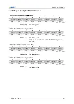
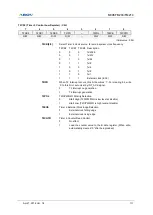
11.5.6.2 Register Description for Timer/Counter 1
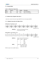
T1ADRH (Timer 1 A data High Register) : BDH
7
6
5
4
3
2
1
0
T1ADRH7
T1ADRH6
T1ADRH5
T1ADRH4
T1ADRH3
T1ADRH2
T1ADRH1
T1ADRH0
R/W
R/W
R/W
R/W
R/W
R/W
R/W
R/W
Initial value : FFH
T1ADRH[7:0]
T1 A Data High Byte
T1ADRL (Timer 1 A Data Low Register) : BCH
7
6
5
4
3
2
1
0
T1ADRL7
T1ADRL6
T1ADRL5
T1ADRL4
T1ADRL3
T1ADRL2
T1ADRL1
T1ADRL0
R/W
R/W
R/W
R/W
R/W
R/W
R/W
R/W
Initial value : FFH
T1ADRL[7:0]
T1 A Data Low Byte
NOTE) Do not write
“0000H” in the T1ADRH/T1ADRL register when
PPG mode
T1BDRH (Timer 1 B Data High Register) : BFH
7
6
5
4
3
2
1
0
T1BDRH7
T1BDRH6
T1BDRH5
T1BDRH4
T1BDRH3
T1BDRH2
T1BDRH1
T1BDRH0
R/W
R/W
R/W
R/W
R/W
R/W
R/W
R/W
Initial value : FFH
T1BDRH[7:0]
T1 B Data High Byte
T1BDRL (Timer 1 B Data Low Register) : BEH
7
6
5
4
3
2
1
0
T1BDRL7
T1BDRL6
T1BDRL5
T1BDRL4
T1BDRL3
T1BDRL2
T1BDRL1
T1BDRL0
R/W
R/W
R/W
R/W
R/W
R/W
R/W
R/W
Initial value : FFH
T1BDRL[7:0]
T1 B Data Low Byte
Summary of Contents for MC96FM204
Page 17: ...MC96FM204 FM214 April 7 2016 Ver 1 8 17 4 Package Diagram Figure 4 1 20 Pin SOP Package ...
Page 18: ...MC96FM204 FM214 18 April 7 2016 Ver 1 8 Figure 4 2 20 Pin TSSOP Package ...
Page 19: ...MC96FM204 FM214 April 7 2016 Ver 1 8 19 Figure 4 3 16 Pin SOP Package ...
Page 20: ...MC96FM204 FM214 20 April 7 2016 Ver 1 8 Figure 4 4 16 Pin TSSOP Package ...


