MC96FM204/FM214
120
April 7, 2016 Ver. 1.8
11.9 8-Bit A/D Converter
11.9.1 Overview
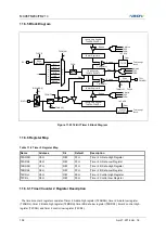
The analog-to-digital(A/D) converter allows conversion of an analog input signal to an corresponding 8-bit digital
value. The A/D module has eight analog inputs, which are multiplexer into one sample and hold.
The output of the sample and hold is the input of the converter which generates the result through successive
approximation. The analog supply voltage is connected to VDD of ladder resistance of A/D module.
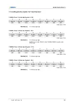
The A/D module has four registers which are the A/D converter control High register (ADCCRH), A/D converter
control low register (ADCCRL), Sample and hold timing data register (SHTDR) and A/D converter data register
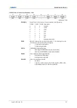
(ADCDR). The channels to be converted are selected by setting ADSEL[3:0]. To execute A/D conversion, ADST
bit should be set
to ‘1’. The register ADCDR contains the results of the A/D conversion. When the conversion is
completed, the result is loaded into the ADCDR, the A/D conversion st
atus bit AFLAG is set to ‘1’, and the A/D
interrupt is set. During
A/D conversion, AFLAG bit is read as ‘0’.
11.9.2 Conversion Timing
When fxx/8 is selected for conversion clock with a 12MHz fxx clock frequency, one clock cycle is 0.66
μs.
SHTDR data is 15. Convert time is 9 clocks, the total conversion rate is calculated as follows:
15 9 clocks = 24 clocks,
24 clock × 0.66
μs = 15.84 μs at 1.5 MHz (12 MHz/8)
NOTE :
The A/D converter needs at least 15
μs for conversion time. So you must set the conversion time more
than 15
μs
.
Summary of Contents for MC96FM204
Page 17: ...MC96FM204 FM214 April 7 2016 Ver 1 8 17 4 Package Diagram Figure 4 1 20 Pin SOP Package ...
Page 18: ...MC96FM204 FM214 18 April 7 2016 Ver 1 8 Figure 4 2 20 Pin TSSOP Package ...
Page 19: ...MC96FM204 FM214 April 7 2016 Ver 1 8 19 Figure 4 3 16 Pin SOP Package ...
Page 20: ...MC96FM204 FM214 20 April 7 2016 Ver 1 8 Figure 4 4 16 Pin TSSOP Package ...


