MC97F6108A User’s manual
19. Memory programming
199
19
Memory programming
MC97F6108A has flash memory to which a program can be written, erased, and overwritten while
mounted on the board. Serial ISP mode and byte-parallel ROM writer mode are supported.
Flash of MC97F6108A features the followings:
Flash Size: 8Kbytes
Single power supply program and erase
Command interface for fast program and erase operation
Up to 10,000 program/erase cycles at typical voltage and temperature for flash memory
Security feature
19.1
Flash control and status registers
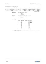
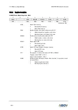
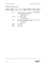
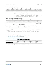
Registers controlling Flash and Data EEPROM are Mode Register (FEMR), Control Register (FECR),
Status Register (FESR), Time Control Register (FETCR), Address Low Register (FEARL), Address
Middle Register (FEARM), address High Register (FEARH) and Data Register (FEDR). They are
mapped to SFR area and can be accessed only in programming mode.
19.1.1
Register map
Table 30. Flash Control and Status Register Map
Name
Address
Dir
Default
Description
FEMR
EAH
R/W
00H
Flash Mode Register
FECR
EBH
R/W
03H
Flash Control Register
FESR
ECH
R/W
80H
Flash Status Register
FETCR
EDH
R/W
00H
Flash Time Control Register
FEARL
F2H
R/W
00H
Flash Address Low Register
FEARM
F3H
R/W
00H
Flash Address Middle Register
FEARH
F4H
R/W
00H
Flash Address High Register
FEDR
F5H
R/W
00H
Flash Data Register

