background image


ACCES I/O Products, Inc. 

MADE IN THE USA 

PCIe-ADIO16-16F Family Manual 


Rev B3d 

All configuration of this device is performed through software; there 
are no jumpers or switches to set. 

C

HAPTER 

5:


PC


I

NTERFACE


This product interfaces with a PC using a PCI Express Gen 2 1×lane 
connection.   
 

C

HAPTER 

6:


I/O


I

NTERFACE


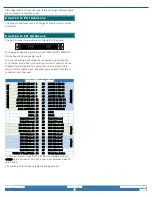
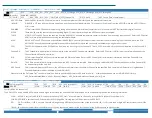
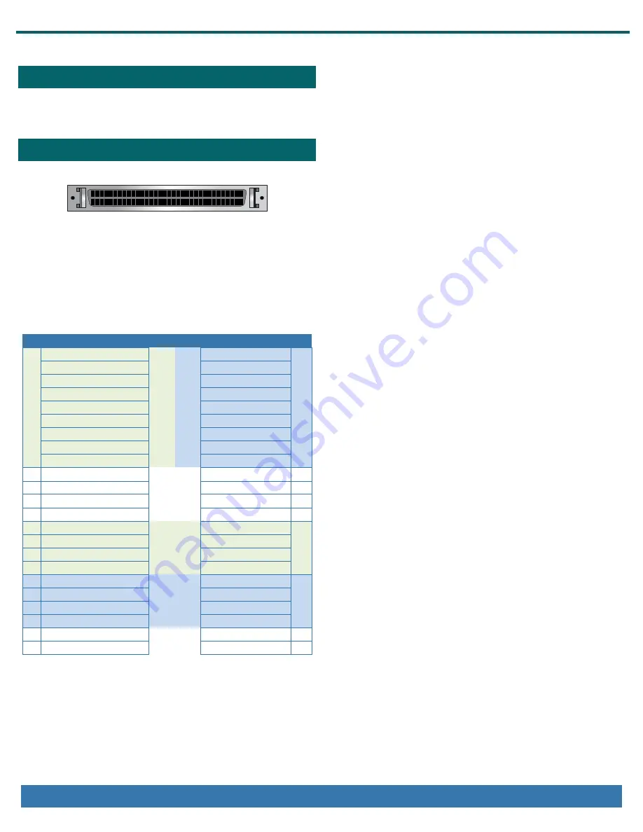
The 68-Pin connector provides all I/O signals for the board: 
 
 
For Singled-Ended analog inputs connect GND to ADC COMMON. 
A Note About Unused Analog Inputs: 
Any unused analog input should be connected to ground with a 

short jumper wire; either in the mating connector cable, or on the 
breakout terminal board. This will reduce / eliminate crosstalk 
which, if left unchecked, can influence measurements of adjacent 

connected

 input channels. 


68-Pin SCSI Female, Latched 

AD

AS

3022 #

S.

E.

 (D

iff.

ADC IN 0 (Ch 0+)  1 

35  ADC IN 1 (Ch 0-) 

AD

AS

3022 #

ADC IN 2 (Ch 1+)  3 

37  ADC IN 3 (Ch 1-) 

ADC IN 4 (Ch 2+)  5 

39  ADC IN 5 (Ch 2-) 

ADC IN 6 (Ch 3+)  7 

41  ADC IN 7 (Ch 3-) 

ADC IN 8 (Ch 4+)  9 

43  ADC IN 9 (Ch 4-) 

ADC IN 10 (Ch 5+)  11 

45  ADC IN 11 (Ch 5-) 

ADC IN 12 (Ch 6+)  13 

47  ADC IN 13 (Ch 6-) 

ADC IN 14 (Ch 7+)  15 

49  ADC IN 15 (Ch 7-) 

ADC1 COMMON  17 

51  ADC2 COMMON 


DAC 0  19 

53  DAC2 


DAC 1  21 

55  DAC 3 


Digital Ground  23 

57  Digital Ground 


Digital Ground  24 

58  Digital Ground 


DIO BitIndex 14  25 

59  DIO BitIndex 15 

Gr

ou

p 1


DIO BitIndex 12  26 

60  DIO BitIndex 13 


DIO BitIndex 10  27 

61  DIO BitIndex 11 


DIO BitIndex 8  28 

62  DIO BitIndex 9 


DIO BitIndex 6  29 

63  DIO BitIndex 7 

Gr

ou

p 0


DIO BitIndex 4  30 

64  DIO BitIndex 5 


DIO BitIndex 2  31 

65  DIO BitIndex 3 


DIO BitIndex 0  32 

66  DIO BitIndex 1 


Digital Ground  33 

67  Digital Ground 


VCCdio

1

 / UserVCCdio  34 

68  Watchdog Active 


1

: VCCio pin outputs fused 3.3VDC @ 0.5A on standard models.   

-VCCIO option converts VCCio into a user input between 1.65VDC 

and 5.5VDC. 
All unlisted pins in the above table are analog ground. 

Summary of Contents for PCIe-ADI12-16

Page 1: ...Sio com 10623 Roselle Street 800 326 1649 http accesio com PCIe ADIO16 16F San Diego CA 92121 1506 USA sales accesio com MADE IN THE USA 16 ANALOG INPUT 4 ANALOG OUTPUT 16 DIGITAL I O FOR PCI EXPRESS...

Page 2: ...A D Scan Start mode optimizes inter channel timing High impedance 8 channel input 1 M 32k FIFO plus DMA for efficient robust data streaming 16 Digital I O pins with flexible secondary functions Four 1...

Page 3: ...0 Ch 0 1 35 ADC IN 1 Ch 0 ADAS3022 1 ADC IN 2 Ch 1 3 37 ADC IN 3 Ch 1 ADC IN 4 Ch 2 5 39 ADC IN 5 Ch 2 ADC IN 6 Ch 3 7 41 ADC IN 7 Ch 3 ADC IN 8 Ch 4 9 43 ADC IN 9 Ch 4 ADC IN 10 Ch 5 11 45 ADC IN 11...

Page 4: ...CH0 1 0 Advanced Sequence Acquires Channel 0 using the gain selected via 18 bits 2 0 Conversion starts will automatically cycle through the channels from CH0 through INx2 0 and each channel is acquir...

Page 5: ...ol bit and status 4 W DAC Control DAC LTC2664 Command Register bits 8 W DAC Waveform Divisor DAC Waveform Points second divisor Base Clock DAC Waveform Rate this register C R ADC Base Clock Frequency...

Page 6: ...to their power on reset state see each ADC Register for more details RST BOARD Writing a 1 will reset the entire device to its power on reset state All RST bits are command bits a 1 causes the reset t...

Page 7: ...llion 125MHz but for broadest compatibility software should always read this register during init and always use the read value when calculating what if any divisor to write to the ADC Rate Divisor re...

Page 8: ...19 D18 D17 D16 D15 D14 D13 D12 D11 D10 D9 D8 D7 D6 D5 D4 D3 D2 D1 D0 Name RSV AIN 15 GAIN2 0 RSV AIN 14 GAIN2 0 RSV AIN 13 GAIN2 0 RSV AIN 12 GAIN2 0 RSV AIN 11 GAIN2 0 RSV AIN 10 GAIN2 0 RSV AIN 9 GA...

Page 9: ...rol 38 for important information about the Channel bits re Differential operation Diff SET indicates the paired ADC Counts were sampled in Differential mode Refer to ADC Control 38 for important infor...

Page 10: ...5 D9 D8 D7 D6 D5 D4 D3 D2 D1 D0 Name WDG UNUSED EXT1 EXT0 LDAC FOF FAF DTO DDONE ADCSTART ADCTRIG UNUSED enEXT1 enEXT0 enLDAC enFOF enFAF enDTO enDDONE enADCSTART enADCTRIG Read IRQ Status to determin...

Page 11: ...as a configurable active edge rising or falling SET the corresponding edgeXXX bit to select rising edge CLEAR the bit for falling edge IOGx SET each IOGx bit to configure the digital I O bits in the a...

Page 12: ...ave introduced a new source of latency the kernel userland division Application code runs in userland which must transition to the kernel in order to perform any hardware operation This transition add...

Page 13: ...all applicable EM interference and emission standards However as they are intended for use installed on motherboards and inside the chassis of industrial PCs important care in the selection of PC and...

Page 14: ...and invoiced COVERAGE FIRST THREE YEARS Returned unit part will be repaired and or replaced at ACCES option with no charge for labor or parts not excluded by warranty Warranty commences with equipmen...

Reviews: