ACCES I/O Products, Inc.
MADE IN THE USA
PCIe-ADIO16-16F Family Manual
4
Rev B3d
C
HAPTER
7:
S
OFTWARE
I
NTERFACE
How to use
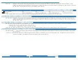
The ADAS3022 is a flexible data acquisition system-on-chip that has numerous features and modes of operation, and additional modes and features are added by our advanced FPGA
design.
This flexibility can seem overwhelming, but we’ve designed our AIOAIO.dll API to make using this ADC simple for 99% of customer use-cases, based on 30+ years of customer feedback.
We strongly recommend you ignore the register details provided in Chapter 7: Software Interface and the discussions regarding low-level control of the ADC in the second half of this
chapter. Instead, simply refer to the AIOAIO Software Reference (.html) manual [link] and the source code to the variety of sample programs provided in the Software Installation
Package [link].
Tip: Taking data from every channel can be as simple as calling “ADC_GetImmediateScanV(0, rangeCode, &data);”, which converts all channels at the specified range and stuffs the data
(as double-precision floating point Voltages) into the data array. This function can be called many thousands of times per second. Please refer to the samples and the software reference
for details on this and other available API functions, including how to acquire 1MHz data via callback or polling.
Advanced Topics
BASIC, ADVANCED, AND NON-SEQUENCED MODES
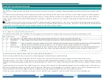
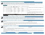
The ADAS3022 uses the SEQ1:0 bits in the +38 and +3C control registers to select between non-sequenced mode, basic sequence mode, and advanced sequence mode.
SEQ1 SEQ0 Mode
Description
0
0
non-Sequenced The ADAS will acquire data from the channel specified in the INx2:0 bits, at the gain specified in the Gain2:0 bits.
0
1
Modify Basic
Sequence
Allows the gain and such to be modified while running a basic sequence, without starting conversions over at CH0.
1
0
Advanced
Sequence
Acquires Channel 0 using the gain selected via +18 bits 2:0. Conversion-starts will automatically cycle through the channels from CH0 through INx2:0,
and each channel is acquired at the per-channel gain set in +18. The sequence repeats, starting at CH0 after INx2:0 is acquired.
1
1
Basic Sequence
Acquires channel 0 using the gain set in Gain2:0. Conversion-starts will automatically cycle through the channels from CH0 through INx2:0, but all
channels are acquired using the gain set in Gain2:0 rather than using the gains from +18. The sequence repeats, starting at CH0 after INx2:0 is
acquired.
SOFTWARE, PERIODIC, AND EXTERNAL START ADC CONVERSION TIMING MODES
ADC data can be acquired periodically, synchronous to an external digital input, or asynchronously via software command.
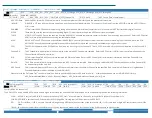
Single, Asynchronous: If the +10 ADC Timing divisor is zero then writing to +38 or +3C with bit 16 set (to 1) will initiate a single ADC Start Event under software control.
Periodic, Asynchronous: If the +10 ADC Timing divisor is non-zero, and the External ADC Trigger Digital Input Secondary function is
not
enabled, writing to +38 with bit 16 set will initiate a
single ADC Start Event, and subsequent events will occur at the rate selected via +10’s divisor. This is “software initiated periodic timed ADC” data. Note: con3C before this write
to +38.
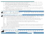
External Trigger, Periodic, Synchronous: If the +10 ADC Timing divisor is non-zero, and the External ADC Trigger Digital Input Secondary function
is
enabled, writing to +38 with bit 16 set
ARMS
the card to begin the periodic collection of ADC data. No data will be collected until the selected edge occurs on the ADC Trigger input. (Refer to +44 for additional details on the
Digital I/O Secondary Functions.) Once triggered, data will be collected until manually stopped by w38 with bit 16 clear (or various resets, etc.).
External Start, Single, Synchronous: The digital input secondary function “ADC Start” can be configured to initiate individual ADC Start Events on a selected edge input.

