$SSHQGL[&
$SSHQGL[&
BIOS POST Checkpoints
BIOS POST Checkpoints
C-1
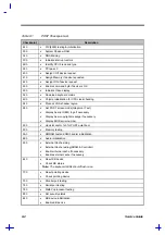
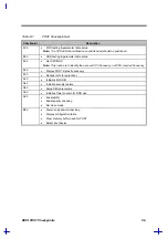
This appendix lists the POST checkpoints of the notebook BIOS.
Table C-1
POST Checkpoint List
Checkpoint
Description
04h
•
Dispatch Shutdown Path
Note: At the beginning of POST, port 64 bit 2 (8042 system flag) is read to determine
whether this POST is caused by a cold or warm boot. If it is a cold boot, a
complete POST is performed. If it is a warm boot, the chip initialization and
memory test is eliminated from the POST routine.
08h
•
Reset PIE, AIE, UIE
Note: These interrupts are disabled in order to avoid any incorrect actions from
happening during the POST routine.
09h
•
Initialize m1531
0Ah
•
Initialize m1533
•
Initialize m7101
10h
•
DMA(8237) testing & initialization
14h
•
System Timer(8254) testing & initialization
18h
•
DRAM refresh cycle testing
•
Set default SS:SP= 0:400
1Ch
•
CMOS shutdown byte test, battery, and check sum
Note: Several parts of the POST routine require the system to be in protected mode.
When returning to real mode from protected mode, the processor is reset,
therefore POST is re-entered. In order to prevent re-initialization of the system,
POST reads the shutdown code stored in location 0Fh in CMOS RAM. Then it
jumps around the initialization procedure to the appropriate entry point.
The CMOS shutdown byte verification assures that CMOS 0Fh area is fine to
execute POST properly.
•
Initialize default CMOS setting if CMOS bad
•
Initialize RTC time base
Note: The RTC has an embedded oscillator that generates a 32.768 KHz frequency. To
initialize the RTC time base, turn on this oscillator and set a divisor to 32768 so
that the RTC can count time correctly
1Dh, 1Eh
•
DRAM type determination
2Ch
•
128K base memory testing
•
Set default SS:SP= 0:400
Note: The 128K base memory area is tested for POST execution. The remaining
memory area is tested later.
20h
•
KB controller(8041/8042) testing
•
KB type determination
•
Write default command byte upon KB type
Summary of Contents for 365 Series
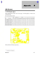
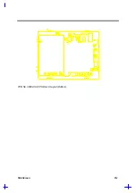
Page 80: ...Silk Screen D 2 PCB No 96532 SA CPU Board Layout Bottom ...
Page 82: ...Mainboard Layout ...
Page 83: ...Bottom ...
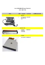
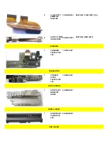
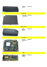
Page 95: ... S S S H Q G S H Q G L L Explored View Diagram ...
Page 96: ......
Page 100: ......
Page 101: ......
Page 115: ......
Page 117: ......
Page 120: ......
Page 122: ......
Page 126: ......

