2-44
Service Guide
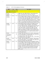
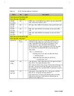
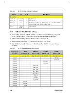
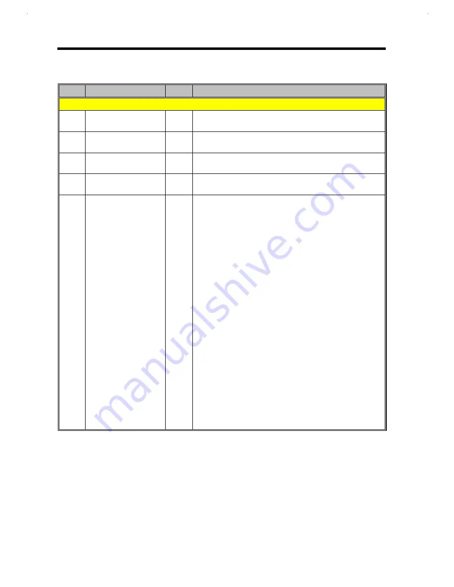
Table 2-10
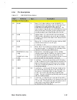
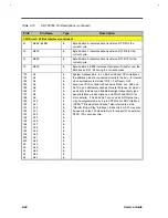
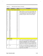
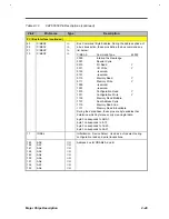
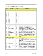
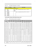
C&T 65550 Pin Descriptions (continued)
Pin#
Pin Name
Type
Description
CPU Direct / VL-Bus Interface (continued)
43
BE0# (BLE#)
In
Byte Enable 0. Indicates data transfer on D7:D0 for the
current cycle.
32
BE1#
In
Byte Enable 1. Indicates data transfer on D15:D8 for the
current cycle.
21
BE2#
In
Byte Enable 2. Indicates data transfer on D23:D16 for the
current cycle.
10
BE3#
In
Byte Enable 3. BE3# indicates that data will transfer over the
data bus on D31 :24 during the current access.
179
180
182
183
185
186
187
188
189
190
191
192
193
194
195
196
197
189
199
200
201
28
29
30
53
54
A2
A3
A4
A5
A6
A7
A8
A9
A10
A11
A12
A13
A14
A15
A16
A17
A18
A19
A20
A21
A22
A23
A24
A25
A26
A27
In
In
In
In
In
In
In
In
In
In
In
In
In
In
In
In
In
In
In
In
In
In
In
In
In
In
System Address Bus. In VL-Bus, and direct CPU interfaces,
the address pins are connected directly to the bus. In internal
clock synthesizer test mode (TS# = 0 at Reset), A24
becomes VCLK out and A25 becomes MCLK out. A26 and
A27 may be alternately used as General Purpose I/O pins or
as Activity Indicator and Enable Backlight respectively (see
panel interface pin descriptions, and FROF and FROC for
more details). If A26 and A27, are used as GPIO pins, they
may be programmed as a 2-pin CRT Monitor DDC interface
(VESA™ "Display Data Channel" also referred to as the
"Monitor Plug-n-Play" interface). Either A26 or A27 may also
be used to output, Composite Sync for support of an external
NTSC / PAL encoder chip.
Summary of Contents for AcerNote Light 370P
Page 6: ...vi ...
Page 26: ...1 8 Service Guide Figure 1 5 Main Board Layout Bottom Side ...
Page 49: ...System Introduction 1 31 1 5 1 3 Power Management Figure 1 14 Power Management Block Diagram ...
Page 55: ...System Introduction 1 37 1 6 System Block Diagram Figure 1 15 System Block Diagram ...
Page 64: ...Major Chips Description 2 7 2 2 5 Pin Diagram Figure 2 4 M1521 Pin Diagram ...
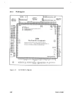
Page 99: ...2 42 Service Guide 2 5 3 Pin Diagram Figure 2 10 C T 65550 Pin Diagram ...
Page 117: ...2 60 Service Guide Figure 2 12 Functional block diagram CardBus Card Interface ...
Page 119: ...2 62 Service Guide Figure 2 14 PCI to CardBus terminal assignments ...
Page 135: ...2 78 Service Guide 2 7 3 Pin Diagram Figure 2 16 NS87336VJG Pin Diagram ...
Page 145: ...2 88 Service Guide 2 8 2 Pin Diagram Figure 2 17 YMF715 Block Diagram ...
Page 185: ...Disassembly and Unit Replacement 4 5 Figure 4 3 Disassembly Sequence Flowchart ...
Page 209: ...B 2 Service Guide ...
Page 210: ...Exploded View Diagram B 3 ...

