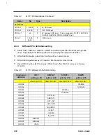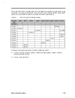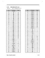
Major Chips Description
2-45
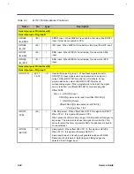
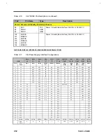
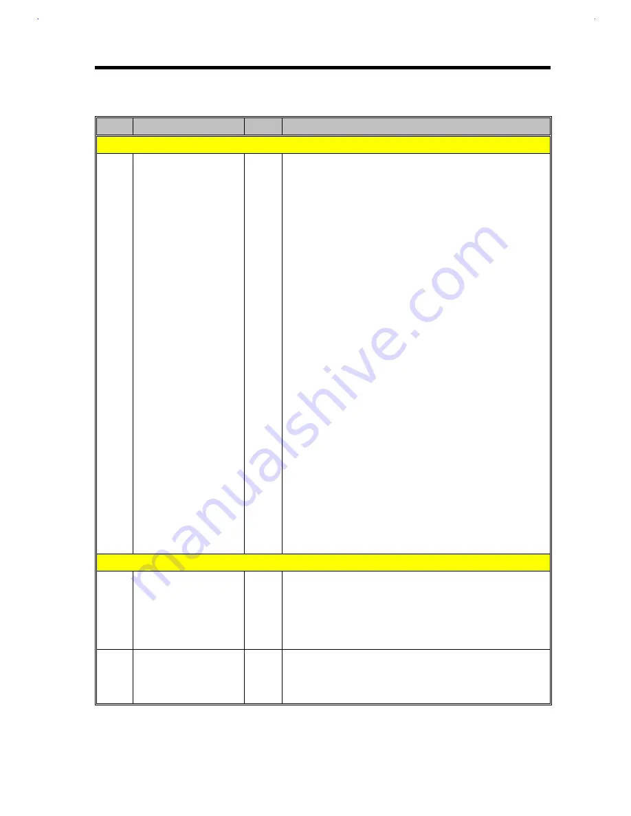
Table 2-10
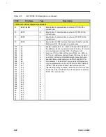
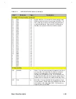
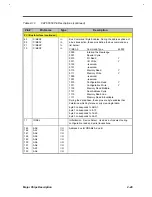
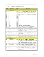
C&T 65550 Pin Descriptions (continued)
Pin#
Pin Name
Type
Description
CPU Direct / VL-Bus Interface (continued)
51
50
49
48
47
46
45
44
41
40
38
37
36
35
34
33
20
19
18
17
16
15
14
13
8
7
6
5
4
3
2
1
D00
D01
D02
D03
D04
D05
D06
D07
D08
D09
D10
D11
D12
D13
D14
D15
D16
D17
D18
D19
D20
D21
D22
D23
D24
D25
D26
D27
D28
D29
D30
D31
I/O
I/O
I/O
I/O
I/O
I/O
I/O
I/O
I/O
I/O
I/O
I/O
I/O
I/O
I/O
I/O
I/O
I/O
I/O
I/O
I/O
I/O
I/O
I/O
I/O
I/O
I/O
I/O
I/O
I/O
I/O
I/O
System Data Bus. In 32-bit CPU Local Bus designs these
data lines connect directly to the processor data lines. On
the VL-Bus they connect to the corresponding buffered or
unbuffered data signal. These pins are tri-stated during
Standby mode (as are all other bus interface outputs).
PCI Bus Interface
207
RESET#
In
Reset. This input sets all signals and registers in the chip to
a known state. All outputs from the chip are tri-stated or
driven to an inactive state. This pin is ignored during
Standby mode (STNDBY# pin low). The remainder of the
system (therefore the system bus) may be powered down if
desired (all bus output pins are tri-stated in Standby mode).
201
CLK
In
Bus Clock. This input provides the timing reference for all
bus transactions. All bus inputs except RESET# and INTA#
are sampled on the rising edge of CLK. CLK may be any
frequency from DC to 33MHz.
Summary of Contents for AcerNote Light 370P
Page 6: ...vi ...
Page 26: ...1 8 Service Guide Figure 1 5 Main Board Layout Bottom Side ...
Page 49: ...System Introduction 1 31 1 5 1 3 Power Management Figure 1 14 Power Management Block Diagram ...
Page 55: ...System Introduction 1 37 1 6 System Block Diagram Figure 1 15 System Block Diagram ...
Page 64: ...Major Chips Description 2 7 2 2 5 Pin Diagram Figure 2 4 M1521 Pin Diagram ...
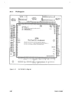
Page 99: ...2 42 Service Guide 2 5 3 Pin Diagram Figure 2 10 C T 65550 Pin Diagram ...
Page 117: ...2 60 Service Guide Figure 2 12 Functional block diagram CardBus Card Interface ...
Page 119: ...2 62 Service Guide Figure 2 14 PCI to CardBus terminal assignments ...
Page 135: ...2 78 Service Guide 2 7 3 Pin Diagram Figure 2 16 NS87336VJG Pin Diagram ...
Page 145: ...2 88 Service Guide 2 8 2 Pin Diagram Figure 2 17 YMF715 Block Diagram ...
Page 185: ...Disassembly and Unit Replacement 4 5 Figure 4 3 Disassembly Sequence Flowchart ...
Page 209: ...B 2 Service Guide ...
Page 210: ...Exploded View Diagram B 3 ...


