2-46
Service Guide
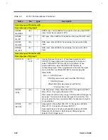
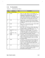
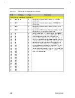
Table 2-10
C&T 65550 Pin Descriptions (continued)
Pin#
Pin Name
Type
Description
PCI Bus Interface (continued)
31
PAR
I/O
Parity. This signal is used to maintain even parity across
AD0-31 and C/BE0-3#. PAR is stable and valid one clock
after the address phase. For data phases, PAR is stable and
valid one clock after either IRDY# is asserted on a write
transaction or TRDY# is asserted on a read transaction.
Once PAR is valid, it remains valid until one clock after the
completion of the current data phase (i.e., PAR has the same
timing as AD0-31 but delayed by one clock). The bus master
drives PAR for address and write data phases; the target
drives PAR for read data phases.
22
FRAME#
In
Cycle Frame. Driven by the current master to indicate the
beginning and duration of an access. Assertion indicates a
bus transaction is beginning (while asserted, data transfers
continue); de-assertion indicates the transaction is in the final
data phase.
23
IRDY#
In
Initiator Ready. Indicates the bus master's ability to complete
the current data phase of the transaction. During a write,
IRDY# indicates valid data is present on AD0-31; during a
read it indicates the master is prepared to accept data. A
data phase is completed on any clock when both IRDY# and
TRDY# are sampled then asserted (wait cycles are inserted
until this occurs).
24
TRDY#
S/TS
Target Ready. Indicates the target's ability to complete the
current data phase of the transaction. During a read, TRDY#
indicates that valid data is present on AD0-31; during a write
it indicates the target is prepared to accept data. A data
phase is completed on any clock when both IRDY# and
TRDY# are sampled then asserted (wait cycles are inserted
until this occurs).
27
STOP#
S/TS
Stop. Indicates the current target is requesting the master to
stop the current transaction
25
DEVSEL#
S/TS
Device Select. Indicates the current target has decoded its
address as the target of the current access
29
PERR# (VCLKOUT)
S/TS
Parity Error. This signal reports data parity errors (except the
Special Cycles where SERR# is used). The PERR# is
Sustained Tri-state. The receiving agent will drive PERR#
active two clocks after detecting a data parity error. PERR#
will be driven high for one clock before being tri-stated as with
all sustained tri-state signals. PERR# will not report status
until the chip has claimed the access by asserting DEVSEL#
and completing the data phase.
Summary of Contents for AcerNote Light 370P
Page 6: ...vi ...
Page 26: ...1 8 Service Guide Figure 1 5 Main Board Layout Bottom Side ...
Page 49: ...System Introduction 1 31 1 5 1 3 Power Management Figure 1 14 Power Management Block Diagram ...
Page 55: ...System Introduction 1 37 1 6 System Block Diagram Figure 1 15 System Block Diagram ...
Page 64: ...Major Chips Description 2 7 2 2 5 Pin Diagram Figure 2 4 M1521 Pin Diagram ...
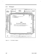
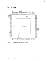
Page 99: ...2 42 Service Guide 2 5 3 Pin Diagram Figure 2 10 C T 65550 Pin Diagram ...
Page 117: ...2 60 Service Guide Figure 2 12 Functional block diagram CardBus Card Interface ...
Page 119: ...2 62 Service Guide Figure 2 14 PCI to CardBus terminal assignments ...
Page 135: ...2 78 Service Guide 2 7 3 Pin Diagram Figure 2 16 NS87336VJG Pin Diagram ...
Page 145: ...2 88 Service Guide 2 8 2 Pin Diagram Figure 2 17 YMF715 Block Diagram ...
Page 185: ...Disassembly and Unit Replacement 4 5 Figure 4 3 Disassembly Sequence Flowchart ...
Page 209: ...B 2 Service Guide ...
Page 210: ...Exploded View Diagram B 3 ...

