Major Chips Description
2-47
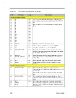
Table 2-10
C&T 65550 Pin Descriptions (continued)
Pin#
Pin Name
Type
Description
PCI Bus Interface (continued)
30
SERR# (MCLKOUT)
OD
System Error. Used to report system errors where the result
will be catastrophic (address parity error, data parity errors
for Special Cycle commands, etc.). This output is actively
driven for a single PCI clock cycle synchronous to CLK and
meets the same setup and hold time requirements as all
other bused signals. SERR# is not driven high by the chip
after being asserted, but is pulled high only by a weak pull-up
provided by the system. Thus, SERR# on the PCI Bus may
take two or three clock periods to fully return to an inactive
state.
179
180
189
183
185
187
189
191
193
180
188
193
194
196
197
198
ROMA0
ROMA1(GPIO3)
ROMA2(GPIO4)
ROMA3(GPIO5)
ROMA4(GPIO6)
ROMA5
ROMA6
ROMA7
ROMA8
ROMA10(GPIO7)
ROMA11
ROMA12
ROMA13
ROMA14
ROMA16
ROMA17
Out
Out
Out
Out
Out
Out
Out
Out
Out
Out
Out
Out
Out
Out
Out
Out
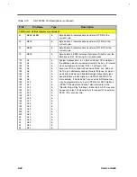
BlOS ROM Address Outputs. See MAD8-15 (pins 170-177)
for BIOS ROM data inputs.
BIOS ROMs are not normally required in portable computer
designs (Graphics System BIOS code is normally included in
the System BIOS ROM). However, the 65550 provides BIOS
ROM interface capability for development systems and add-in
card Flat Panel Graphics Controllers.
Since the PCI Bus specifications require only one load on the
bus for the entire graphics subsystem, the BlOS ROM
interface is through the chip. In the VL-Bus mode. the BIOS
ROM interface can be an external circuit on the ISA Bus
connector that does not require pins on the chip.
200
ROMOE#
Out
BlOS ROM Output Enable.
199
Reserved
In
This pin is always an input (A20 for VL-Bus, reserved for
future use on PCI Bus). To avoid abnormal Vcc current due
to a floating input for a PCI Bus, use a 10K resistor to ground
to pull this pin low..
28
Reserved
In
This pin is always an input (A23 for VL-Bus, reserved for
future use on PCI Bus). To avoid abnormal Vcc current due
to a floating input for a PCI Bus, use a l0K resistor to ground
to pull this pin low.
Summary of Contents for AcerNote Light 370P
Page 6: ...vi ...
Page 26: ...1 8 Service Guide Figure 1 5 Main Board Layout Bottom Side ...
Page 49: ...System Introduction 1 31 1 5 1 3 Power Management Figure 1 14 Power Management Block Diagram ...
Page 55: ...System Introduction 1 37 1 6 System Block Diagram Figure 1 15 System Block Diagram ...
Page 64: ...Major Chips Description 2 7 2 2 5 Pin Diagram Figure 2 4 M1521 Pin Diagram ...
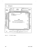
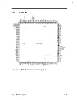
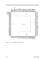
Page 99: ...2 42 Service Guide 2 5 3 Pin Diagram Figure 2 10 C T 65550 Pin Diagram ...
Page 117: ...2 60 Service Guide Figure 2 12 Functional block diagram CardBus Card Interface ...
Page 119: ...2 62 Service Guide Figure 2 14 PCI to CardBus terminal assignments ...
Page 135: ...2 78 Service Guide 2 7 3 Pin Diagram Figure 2 16 NS87336VJG Pin Diagram ...
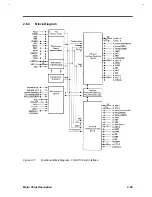
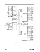
Page 145: ...2 88 Service Guide 2 8 2 Pin Diagram Figure 2 17 YMF715 Block Diagram ...
Page 185: ...Disassembly and Unit Replacement 4 5 Figure 4 3 Disassembly Sequence Flowchart ...
Page 209: ...B 2 Service Guide ...
Page 210: ...Exploded View Diagram B 3 ...


