Major Chips Description
2-51
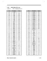
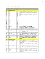
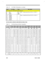
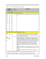
Table 2-10
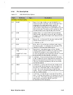
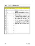
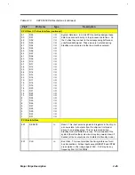
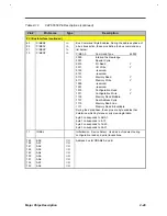
C&T 65550 Pin Descriptions (continued)
Pin#
Pin Name
Type
Description
Display Memory Interface
162
163
164
165
166
167
168
169
170
171
172
173
174
175
176
177
MAD0
MAD1
MAD2 (CFG10)
MAD3 (CFG11)
MAD4 (CFG12)
MAD5 (CFG13)
MAD6 (CFG14)
MAD7 (CFG15)
MAD8 (PCI ROMD0)
MAD9 (PCI ROMD1)
MAD10 (PCI ROMD2)
MAD11 (PCI ROMD3)
MAD12 (PCI ROMD4)
MAD13 (PCI ROMD5)
MAD14 (PCI ROMD6)
MAD15 (PCI ROMD7)
I/O
I/O
I/O
I/O
I/O
I/O
I/O
I/O
I/O
I/O
I/O
I/O
I/O
I/O
I/O
I/O
Memory data bus for DRAM A. (lower 512KB of display
memory)
MAD2-7 are latched into XR71 register on reset for use as
additional configuration inputs (CFG10-12 are reserved by
software for input of panel ID). These bits have no other
internal hardware configuration function.
PCI Bus: MAD8-15 are used as BIOS ROM Data inputs
during system startup (i.e., before the system enables the
graphics controller memory interface). See also pins 179-199
(in PCI Bus interface pin descriptions section) for BIOS ROM
address and ROAM Chip Select outputs. In the VL-Bus
mode, the BIOS ROM interface can be an external circuit on
the ISA Bus connector.
127
128
129
130
131
132
133
134
135
136
137
138
140
141
143
144
MBD0
MBD1
MBD2
MBD3
MBD4
MBDS
MBD6
MBD7
MBD8
MBD9
MBD10
MBD11
MBD12
MBD13
MBD14
MBD15
I/O
I/O
I/O
I/O
I/O
I/O
I/O
I/O
I/O
I/O
I/O
I/O
I/O
I/O
I/O
I/O
Memory data bus for DRAM B (upper 512KB)
106
107
109
110
111
112
113
114
115
116
117
118
119
120
121
122
MCD0 (VB2) (EVID#)
MCDI (VB3) (VP0)
MCD2 (VB4) (VP1)
MCD3 (VB5) (VP2)
MCD4 (VB6) (VP3)
MCD5 (VB7) (VP4)
MCD6 (VG2) (VP5)
MCD7 (VG3) (VP6)
MCD8 (VG4) (VP7)
MCD9 (VG5) (VP8)
MCD10 (VG6) (VP9)
MCD11(VG7) (VP10)
MCD12(VR2) (GRDY)
MCD13(VR3) (VP11)
MCD14(VR4) (VP12)
MCD15 (VR5) (VP13)
Memory data bus for DRAM C (Frame Buffer). When a frame
buffer DRAM is not required, this bus may be used to input up
to 18 bits of RGB data from an external PC-Video subsystem
or 16 bits of RGB from an external VAFC interface. Note that
this configuration also provides additional panel outputs so
that a video input port may be implemented along with a 24-
bit true-color TFT panel (TFT panels never need DRAMC). In
VAFC interface mode, pin 106 is the VAFC "Enable Video"
Input. The external VAFC interface drives this pin low to
indicate data input on the VP0-15. EVID# is ignored
(essentially reserved) in the 65550 (VAFC data is always
expected as inputs). In VAFC mode, pin 119 is ''Graphics
System Ready" out and is always driven high.
Summary of Contents for AcerNote Light 370P
Page 6: ...vi ...
Page 26: ...1 8 Service Guide Figure 1 5 Main Board Layout Bottom Side ...
Page 49: ...System Introduction 1 31 1 5 1 3 Power Management Figure 1 14 Power Management Block Diagram ...
Page 55: ...System Introduction 1 37 1 6 System Block Diagram Figure 1 15 System Block Diagram ...
Page 64: ...Major Chips Description 2 7 2 2 5 Pin Diagram Figure 2 4 M1521 Pin Diagram ...
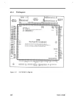
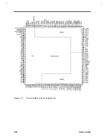
Page 99: ...2 42 Service Guide 2 5 3 Pin Diagram Figure 2 10 C T 65550 Pin Diagram ...
Page 117: ...2 60 Service Guide Figure 2 12 Functional block diagram CardBus Card Interface ...
Page 119: ...2 62 Service Guide Figure 2 14 PCI to CardBus terminal assignments ...
Page 135: ...2 78 Service Guide 2 7 3 Pin Diagram Figure 2 16 NS87336VJG Pin Diagram ...
Page 145: ...2 88 Service Guide 2 8 2 Pin Diagram Figure 2 17 YMF715 Block Diagram ...
Page 185: ...Disassembly and Unit Replacement 4 5 Figure 4 3 Disassembly Sequence Flowchart ...
Page 209: ...B 2 Service Guide ...
Page 210: ...Exploded View Diagram B 3 ...

