2-52
Service Guide
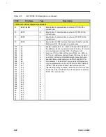
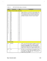
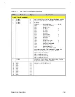
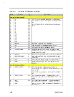
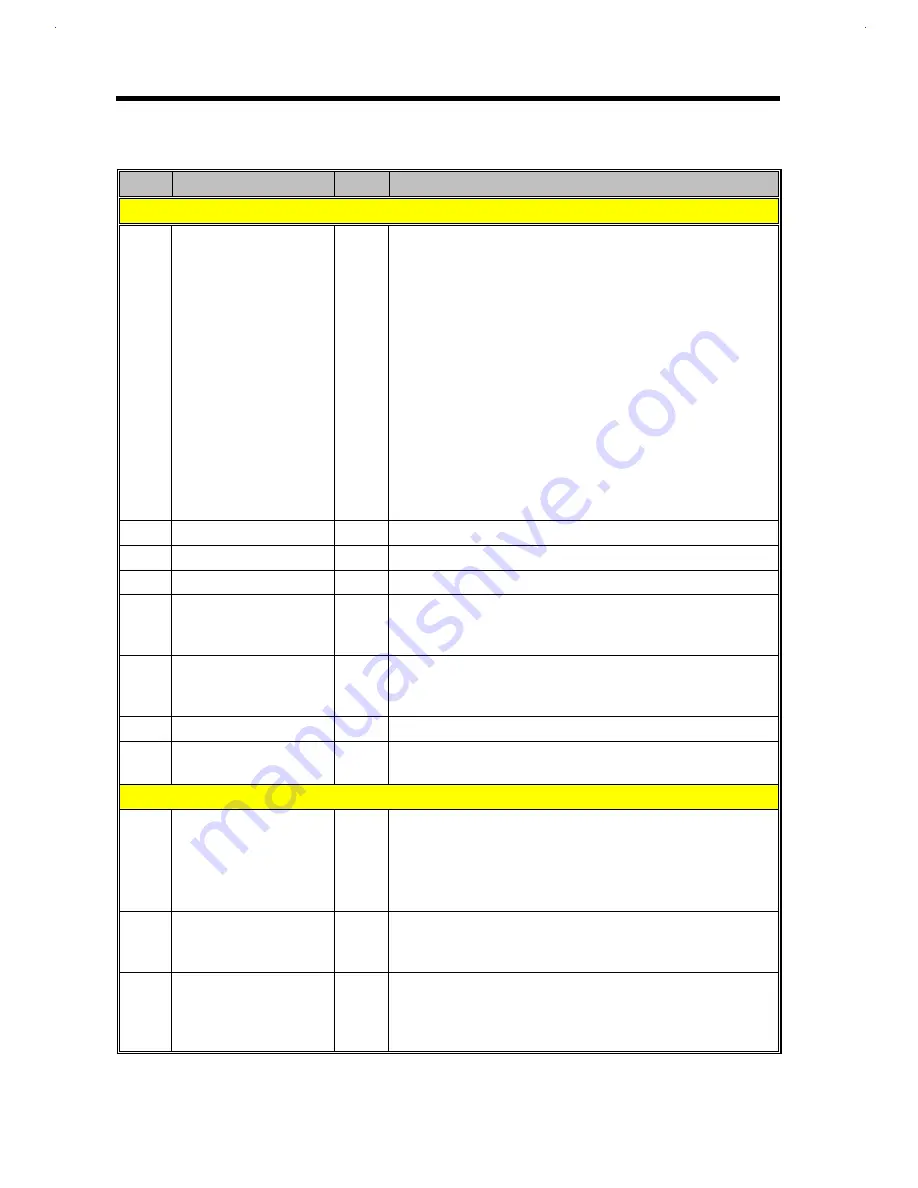
Table 2-10
C&T 65550 Pin Descriptions (continued)
Pin#
Pin Name
Type
Description
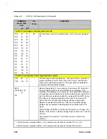
Flat Panel Display Interface
71
72
73
74
75
76
78
79
81
82
83
84
85
86
87
88
P0
P1
P2
P3
P4
P5
P6
P7
P8
P9
P10
P11
P12
P13
P14
P15
Out
Out
Out
Out
Out
Out
Out
Out
Out
Out
Out
Out
Out
Out
Out
Out
8, 9, 12, or 16-bit flat panel data output. 18-bit and 24-bit
panel interfaces may also be supported (see CA0-7 for P16-
23).
Refer to Table 2-7 for the configurations for various panel
types.
70
SHFCLK
Out
Shift Clock. Pixel clock for flat panel data.
67
FLM
Out
First Line Marker. Flat Panel equivalent of VSYNC.
68
LP
Out
Latch Pulse. Flat Panel equivalent of HSYNC.
69
M (DE) (BLANK#)
Out
M signal for panel AC drive control. (may also be called
ACDCLK). May also be configured as BLANK# or as Display
Enable (DE) for TFT Panels.
62
61
ENAVDD
ENAVEE (ENABKL)
I/O
I/O
Power sequencing controls. Power sequencing controls. for
panel driver electronics voltage VDD and panel LCD bias
voltage VEE
53
ACTI
I/O
Activity Indicator. May be configured for other functions
54
ENBKL
I/O
Enable Backlight Outputs. May be configured for other
functions
Flat Panel Display Interface
65
HYSNC (CSYNC)
Out
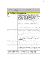
CRT Horizontal Sync (polarity is programmable) or
"Composite Sync" for support of various external NTSC / PAL
encoder chips.
Note CSYNC can be set to output on the ACTI or ENABKL
pins.
64
VSYNC (VISINT)
Out
CRT Vertical Sync (polarity is programmable) or "Vsync
Interval" for support of various external NTSC / PAL encoder
chips.
60
58
57
RED
GREEN
BLUE
Out
CRT analog video outputs from the internal color palette
DAC. The DAC is designed for a 37.5
Ω
equivalent load on
each pin (e.g. 75
Ω
resistor on the board, in parallel with the
75
Ω
CRT load.
Summary of Contents for AcerNote Light 370P
Page 6: ...vi ...
Page 26: ...1 8 Service Guide Figure 1 5 Main Board Layout Bottom Side ...
Page 49: ...System Introduction 1 31 1 5 1 3 Power Management Figure 1 14 Power Management Block Diagram ...
Page 55: ...System Introduction 1 37 1 6 System Block Diagram Figure 1 15 System Block Diagram ...
Page 64: ...Major Chips Description 2 7 2 2 5 Pin Diagram Figure 2 4 M1521 Pin Diagram ...
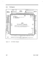
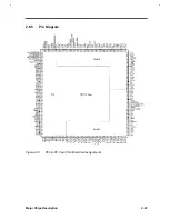
Page 99: ...2 42 Service Guide 2 5 3 Pin Diagram Figure 2 10 C T 65550 Pin Diagram ...
Page 117: ...2 60 Service Guide Figure 2 12 Functional block diagram CardBus Card Interface ...
Page 119: ...2 62 Service Guide Figure 2 14 PCI to CardBus terminal assignments ...
Page 135: ...2 78 Service Guide 2 7 3 Pin Diagram Figure 2 16 NS87336VJG Pin Diagram ...
Page 145: ...2 88 Service Guide 2 8 2 Pin Diagram Figure 2 17 YMF715 Block Diagram ...
Page 185: ...Disassembly and Unit Replacement 4 5 Figure 4 3 Disassembly Sequence Flowchart ...
Page 209: ...B 2 Service Guide ...
Page 210: ...Exploded View Diagram B 3 ...


