Major Chips Description
2-55
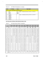
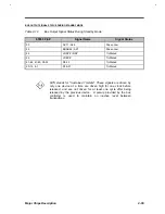
BUS OUTPUT SIGNAL STATUS DURING STANDBY MODE
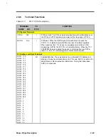
Table 2-12
Bus Output Signal Status During Standby Mode
65550 Pin#
Signal Name
Signal Status
53
ACTI / A26
Driven Low
54
EBABKL / A27
Driven Low
24
LRDY# / RDY
Tri-Stated
25
LDEV#
Tri-Stated
51-44, 41-40, 38-33
D0-15
Tri-Stated
20-13, 8-1
D16-31
Tri-Stated
S/TS stands for "Sustained Tri-state". These signals are driven by
only one device at a time are driven high for one clock before
released, and are not driven for at least one cycle after being
released by the previous device. A pull-up provided by the bus
controller is used to maintain an inactive level between
transactions.
Summary of Contents for AcerNote Light 370P
Page 6: ...vi ...
Page 26: ...1 8 Service Guide Figure 1 5 Main Board Layout Bottom Side ...
Page 49: ...System Introduction 1 31 1 5 1 3 Power Management Figure 1 14 Power Management Block Diagram ...
Page 55: ...System Introduction 1 37 1 6 System Block Diagram Figure 1 15 System Block Diagram ...
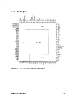
Page 64: ...Major Chips Description 2 7 2 2 5 Pin Diagram Figure 2 4 M1521 Pin Diagram ...
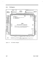
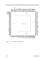
Page 99: ...2 42 Service Guide 2 5 3 Pin Diagram Figure 2 10 C T 65550 Pin Diagram ...
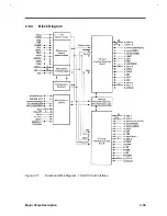
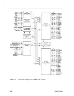
Page 117: ...2 60 Service Guide Figure 2 12 Functional block diagram CardBus Card Interface ...
Page 119: ...2 62 Service Guide Figure 2 14 PCI to CardBus terminal assignments ...
Page 135: ...2 78 Service Guide 2 7 3 Pin Diagram Figure 2 16 NS87336VJG Pin Diagram ...
Page 145: ...2 88 Service Guide 2 8 2 Pin Diagram Figure 2 17 YMF715 Block Diagram ...
Page 185: ...Disassembly and Unit Replacement 4 5 Figure 4 3 Disassembly Sequence Flowchart ...
Page 209: ...B 2 Service Guide ...
Page 210: ...Exploded View Diagram B 3 ...


