Major Chips Description
2-69
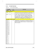
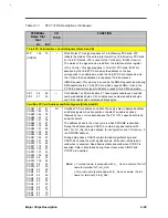
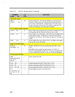
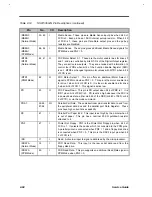
Table 2-13
PCI1131 Pin Descriptions (Continued)
TERMINAL
Name Slot
Slot
I/O
TYPE
FUNCTION
A+ B
≠≠
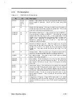
1 6-bit PC Card Interface Control Signals (Slots A and B)
WP
139 73
(IOIS16)
I
Write Protect. This signal applies to 16-bit Memory PC Cards. WP
reflects the status of the write-protect switch on 16-bitmemory PC Cards.
For 16-bit l/O cards, WP is used for the 16-bit port ( IOIS16) function.
The status of the signal can be read from the interface status register.
(I/O is 16 bits). This signal applies to 16-bit l/O PC Cards. IOIS16 is
asserted by the 16-bit PC Card when the address on the bus
corresponds to an address to which the 16-bit PC Card responds, and
the I /O port that is addressed is capable of 16-bit accesses.
(DMA Request). This pin may be used as the DMA Request signal during
DMA operations to a 16-bit PC Card which supports DMA. If used, the
PC Card asserts this signal to indicate a request for a DMA operation.
CE1
94 28
CE2
97 30
O
Card Enable 1 and Card Enable 2. These signals enable even and odd
numbered address bytes. CE1 enables even numbered address bytes,
and CE2 enables odd numbered address bytes.
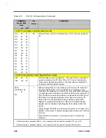
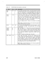
CardBus PC Card Address and Data Signals (Slots A and B)
CAD31 147 81
CAD30 145 79
CAD29 144 78
CAD28 142 77
CAD27 141 76
CAD26 133 67
CAD25 132 66
CAD24 131 65
CAD23 128 62
CAD22 126 60
CAD21 123 57
CAD19 121 55
CAD18 119 54
CAD17 118 53
CAD16 103 37
CAD15 101 35
CAD14 102 36
CAD13 99 33
CAD12 100 34
CAD11 98 32
CAD10 97 30
CAD9
95 29
CAD8
93 27
CAD7
92 26
CAD6
89 23
CAD5
90 24
CAD4
87 20
CAD3
88 21
CAD2
84 18
CAD1
85 19
CAD0
83 17
I/O
CardBus PC Card address and data These pins are multiplexed address
and data signals A bus transaction consists of an address phase
followed by one or more data phases The PCI 1131 supports both read
and write bursts.
The address phase is the clock cycle in which CFRAME is asserted.
During the address phase, CAD31-0 contain a physical address (32-
bits). For l/O, this is a byte address; for configuration and I/O memory, it
is a DWORD address.
During data phases, CAD74 contain the least significant byte and
CAD31-24 contain the most significant byte. Write data is stable and
valid when is asserted. Read data is stable and valid when CTRDY is
asserted. Data is transferred during those clocks when CIRDY and
CTRDY are asserted.
Note:
+
Terminal name is preceded with A_. As an example, the full
name for terminal 121 is A_A25.
≠
Terminal name is preceded with B_. As an example, the full
name for terminal 55 is B_A25.
Summary of Contents for AcerNote Light 370P
Page 6: ...vi ...
Page 26: ...1 8 Service Guide Figure 1 5 Main Board Layout Bottom Side ...
Page 49: ...System Introduction 1 31 1 5 1 3 Power Management Figure 1 14 Power Management Block Diagram ...
Page 55: ...System Introduction 1 37 1 6 System Block Diagram Figure 1 15 System Block Diagram ...
Page 64: ...Major Chips Description 2 7 2 2 5 Pin Diagram Figure 2 4 M1521 Pin Diagram ...
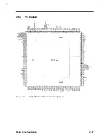
Page 99: ...2 42 Service Guide 2 5 3 Pin Diagram Figure 2 10 C T 65550 Pin Diagram ...
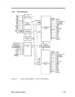
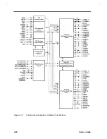
Page 117: ...2 60 Service Guide Figure 2 12 Functional block diagram CardBus Card Interface ...
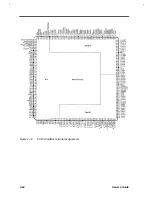
Page 119: ...2 62 Service Guide Figure 2 14 PCI to CardBus terminal assignments ...
Page 135: ...2 78 Service Guide 2 7 3 Pin Diagram Figure 2 16 NS87336VJG Pin Diagram ...
Page 145: ...2 88 Service Guide 2 8 2 Pin Diagram Figure 2 17 YMF715 Block Diagram ...
Page 185: ...Disassembly and Unit Replacement 4 5 Figure 4 3 Disassembly Sequence Flowchart ...
Page 209: ...B 2 Service Guide ...
Page 210: ...Exploded View Diagram B 3 ...

