2-70
Service Guide
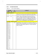
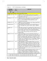
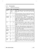
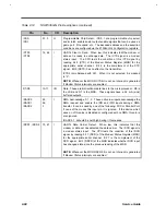
Table 2-13
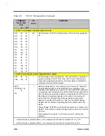
PCI1131 Pin Descriptions (Continued)
TERMINAL
Name Slot
Slot
I/O
TYPE
FUNCTION
A+ B
≠≠
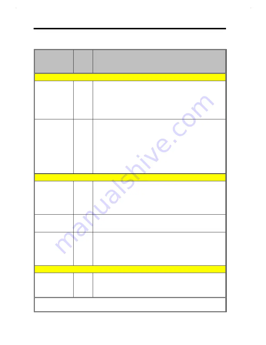
CardBus PC Card Address and Data Signals (Slots A and B)
CC/BE0 94 28
CC/BE1 104 39
CC/BE2 117 52
CC/BE3 130 63
I/O
CardBus PC Card Command and Byte Enables. These signals are
multiplexed on the same pin. During the address phase of the
transaction, CC/BE3 0 define the bus command. During the data I/O
phase transaction, CC/BE3-0 are used as Byte Enables. Byte Enables
are valid during the entire data phase and determine the byte lanes that
will carry the data. CC/BE0 applies to byte 0, CC/BE3 applies to byte 1,
CC/EE2 applies to byte 2, and CC/BE3 applies to byte 3.
CPAR
106 41
I/O
CardBus PC Card Parity. Even parity across CAD3 1-0 and CC/ES3-O is
calculated and driven by this signal. CPAR is stable and valid for one
clock after the address phase. For Data phases, CPAR is stable and
valid one clock after either CIRDY is asserted on a write transaction or
CTRDY is asserted on a read transaction. Once CPAR is valid, it
remains valid for one clock after the completion of the current data
phase. Note: CPAR has the same timing as CAD31-0 but delays by one
clock. When the PCI 1131 is acting as an initiator, it will drive CPAR for
address and write data phases; and when acting as a target, the
PCI1131 will drive CPAR for read data phases.
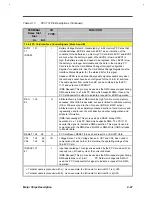
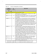
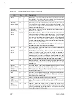
CardBus PC Card Interface System Signals (Slots A and B)
CCLK
112 48
O
CardBus PC Card Clock. This signal provides synchronous timing for all
transactions on the CardBus PC Card interface. All signals except MST
(upon assertion) CCLKRUN, CIST, CSTSCHG, CAUDIO, CCD2-1, and
CVS2-1 are sampled on the rising edge of the clock, and all timing
parameters are defined with the rising edge of this signal. The CardBus
clock operates at 33 MHz, but it can be stopped in the low state.
CCLKRUN 139 73
I/O
CardBus PC Card Clock Run. This signal is used by a CardBus PC Card
to request an increase in the CCLK frequency, and by the PCI 1131 to
indicate that the CCLK frequency will be decreased.
CRST
124
58
O
CardBus PC Card Reset. This signal is used to bring CardBus PC Card
specific registers, sequencers, and signals to a consistent state. When
ZMT is asserted, all CardBus PC Card signals must be driven to high
impedance state, but the PCI 1131 will drive these signals to a valid logic
level. Assertion may be asynchronous for the CCLK but deassertion
must be synchronous to the CCLK.
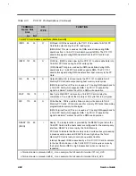
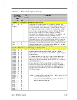
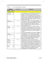
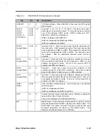
CardBus PC Card Interface Control Signals (Slots A and B)
CCD1
82 16
CCD2
140 74
I
CardBus Detect 1 and CardBus Detect 2. CCD1 and CCD2 are used in
conjunction with CVS1 and CVS2 to determine the type and voltage of
the CardBus PC Card. The signal status is available
by reading the Interface Status Register
+
Terminal name is preceded with A_. As an example, the full name for terminal 121 is A_A25.
≠
Terminal name is preceded with B_. As an example, the full name for terminal 55 is B_A25.
Summary of Contents for AcerNote Light 370P
Page 6: ...vi ...
Page 26: ...1 8 Service Guide Figure 1 5 Main Board Layout Bottom Side ...
Page 49: ...System Introduction 1 31 1 5 1 3 Power Management Figure 1 14 Power Management Block Diagram ...
Page 55: ...System Introduction 1 37 1 6 System Block Diagram Figure 1 15 System Block Diagram ...
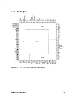
Page 64: ...Major Chips Description 2 7 2 2 5 Pin Diagram Figure 2 4 M1521 Pin Diagram ...
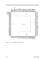
Page 99: ...2 42 Service Guide 2 5 3 Pin Diagram Figure 2 10 C T 65550 Pin Diagram ...
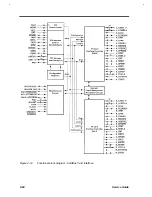
Page 117: ...2 60 Service Guide Figure 2 12 Functional block diagram CardBus Card Interface ...
Page 119: ...2 62 Service Guide Figure 2 14 PCI to CardBus terminal assignments ...
Page 135: ...2 78 Service Guide 2 7 3 Pin Diagram Figure 2 16 NS87336VJG Pin Diagram ...
Page 145: ...2 88 Service Guide 2 8 2 Pin Diagram Figure 2 17 YMF715 Block Diagram ...
Page 185: ...Disassembly and Unit Replacement 4 5 Figure 4 3 Disassembly Sequence Flowchart ...
Page 209: ...B 2 Service Guide ...
Page 210: ...Exploded View Diagram B 3 ...

