2-84
Service Guide
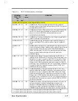
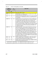
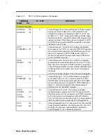
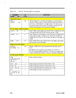
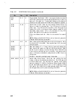
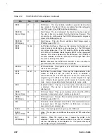
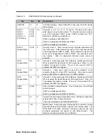
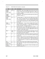
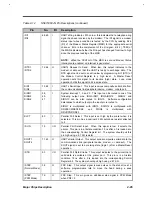
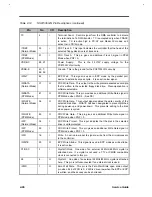
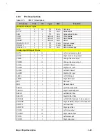
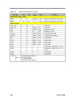
Table 2-14
NS87336VJG Pin Descriptions (continued)
Pin
No.
I/O
Description
/MSEN0
/MSEN1
(Normal Mode)
50, 49
I
Media Sense. These pins are Media Sense input pins when bit 0 of
FCR is 0. Each pin has a 10 K
Ω
internal pull-up resistor. When bit 0
of FCR is 1, these pins are Data Rate output pins and the pull-up
resistors are disabled.
/MSEN0
/MSEN1
(PPM Mode)
86, 84
I
Media Sense. These pins gives additional Media Sense signals for
PPM Mode and PNF = 0.
/MTR0
/MTR1
(Normal Mode)
44, 41
O
FDC Motor Select 0, 1. These are the motor enable lines for drives 0
and 1, and are controlled by bits D7-D4 of the Digital Output register.
They are active low outputs. They are encoded with information to
control four FDDs when bit 4 of the Function Enable Register (FER)
is set. MTR0 exchanges logical motor values with MTR1 when bit 4
of FCR is set.
/MTR1
(PMM Mode)
82
O
FDC Motor Select 1. This pin offers an additional Motor Select 1
signal in PPM mode when PNF = 0. This pin is the motor enable line
for drive 1 when bit 4 of FCR is 0. It is the motor enable line for drive
0 when bit 4 of FCR 1. This signal is active low
PD
43
O
FDC Power Down. This pin is PD output when bit 4 of PMC is 1. It is
/DR1 when bit 4 of PMC is 0. PD is active high whenever the FDC is
in power-down state, either via bit 6 of the DSR (or bit 3 of FER, or bit
0 of PTR), or via the mode command.
PD0-7
92-89,
87-84
I/O
Parallel Port Data. These bidirectional pins transfer data to and from
the peripheral data bus and the parallel port Data Register. These
pins have high current drive capability.
PE
81
I
Parallel Port Paper End. This input is set high by the printer when it
is out of paper. This pin has a nominal 25 K
Ω
pull-down resistor
attached to it.
PNF
47
I
Printer Not Floppy. PNF is the Printer Not Floppy pin when bit 2 of
FCR is 1. It selects the device which is connected to the PPM pins.
A parallel printer is connected when PNF = 1 and a floppy disk drive
is connected when PNF = 0. This pin is the DRV2 input pin when bit
2 of FCR is 0.
/RD
17
I
Read. Active low input to signal a data read by the microprocessor.
/RDATA
(Normal Mode)
33
I
FDD Read Data. This input is the raw serial data read from the
floppy disk drive.
/RDATA
(PPM Mode)
89
I
FDD Read Data. This pin supports an additional Read Data signal in
PPM Mode when PNF = 0.
Summary of Contents for AcerNote Light 370P
Page 6: ...vi ...
Page 26: ...1 8 Service Guide Figure 1 5 Main Board Layout Bottom Side ...
Page 49: ...System Introduction 1 31 1 5 1 3 Power Management Figure 1 14 Power Management Block Diagram ...
Page 55: ...System Introduction 1 37 1 6 System Block Diagram Figure 1 15 System Block Diagram ...
Page 64: ...Major Chips Description 2 7 2 2 5 Pin Diagram Figure 2 4 M1521 Pin Diagram ...
Page 99: ...2 42 Service Guide 2 5 3 Pin Diagram Figure 2 10 C T 65550 Pin Diagram ...
Page 117: ...2 60 Service Guide Figure 2 12 Functional block diagram CardBus Card Interface ...
Page 119: ...2 62 Service Guide Figure 2 14 PCI to CardBus terminal assignments ...
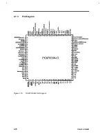
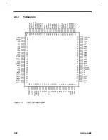
Page 135: ...2 78 Service Guide 2 7 3 Pin Diagram Figure 2 16 NS87336VJG Pin Diagram ...
Page 145: ...2 88 Service Guide 2 8 2 Pin Diagram Figure 2 17 YMF715 Block Diagram ...
Page 185: ...Disassembly and Unit Replacement 4 5 Figure 4 3 Disassembly Sequence Flowchart ...
Page 209: ...B 2 Service Guide ...
Page 210: ...Exploded View Diagram B 3 ...


