2-6
Service Guide
2.2.4
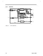
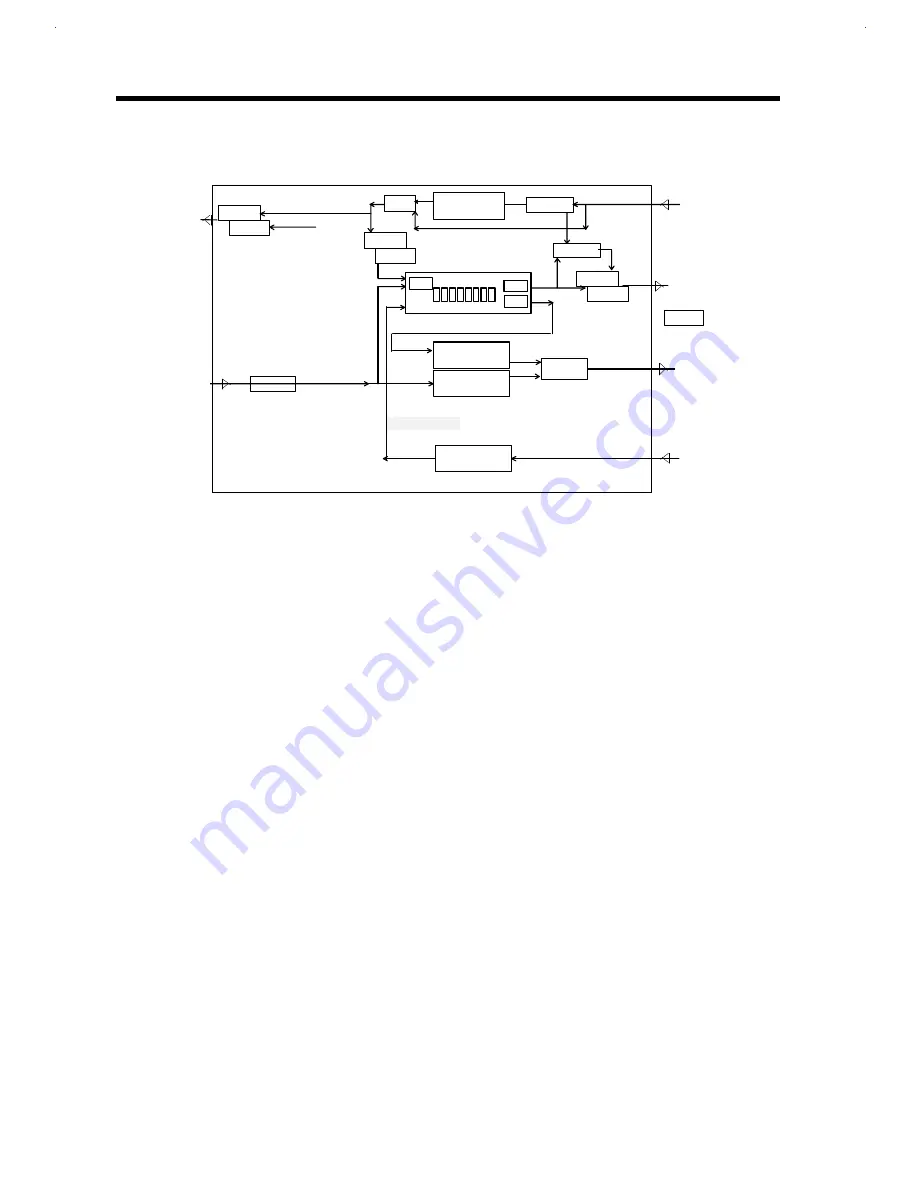
Data Path
E C C
64-bit
S W A P
H D _
O U T
64-bit
S W A P
6 D W O R D
5 D W O R D
6 D W O R D
M U X
P C I _ O U T
P C I _ I N
P_IN[31:0]
P B _ O U T [ 6 3 : 0 ]
64-bit
HDIN[63:0]
M U X
72-bit
E C C
72-bit
S W A P
8 Q W O R D
M U X
M U X
M U X
MDIN[63:0]
PCI_IN
MD_IN[63:0]
PB_IN[63:0]
H D _ I N
S W A P
H / L D W s w a p
for 32-bit DRAM
M D _ O U T
M 1 5 2 1
M D _ I N
ECC partial
W-R path
Figure 2-3
M1521 Data Path
Summary of Contents for AcerNote Light 370P
Page 6: ...vi ...
Page 26: ...1 8 Service Guide Figure 1 5 Main Board Layout Bottom Side ...
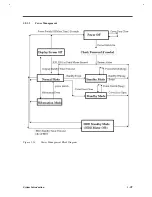
Page 49: ...System Introduction 1 31 1 5 1 3 Power Management Figure 1 14 Power Management Block Diagram ...
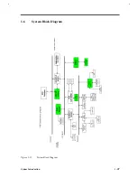
Page 55: ...System Introduction 1 37 1 6 System Block Diagram Figure 1 15 System Block Diagram ...
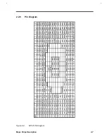
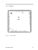
Page 64: ...Major Chips Description 2 7 2 2 5 Pin Diagram Figure 2 4 M1521 Pin Diagram ...
Page 99: ...2 42 Service Guide 2 5 3 Pin Diagram Figure 2 10 C T 65550 Pin Diagram ...
Page 117: ...2 60 Service Guide Figure 2 12 Functional block diagram CardBus Card Interface ...
Page 119: ...2 62 Service Guide Figure 2 14 PCI to CardBus terminal assignments ...
Page 135: ...2 78 Service Guide 2 7 3 Pin Diagram Figure 2 16 NS87336VJG Pin Diagram ...
Page 145: ...2 88 Service Guide 2 8 2 Pin Diagram Figure 2 17 YMF715 Block Diagram ...
Page 185: ...Disassembly and Unit Replacement 4 5 Figure 4 3 Disassembly Sequence Flowchart ...
Page 209: ...B 2 Service Guide ...
Page 210: ...Exploded View Diagram B 3 ...

