2-8
Service Guide
2.2.6
Signal Descriptions
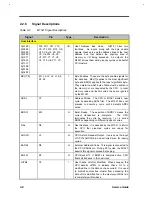
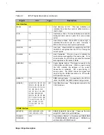
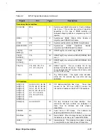
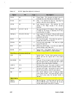
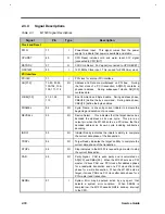
Table 2-2
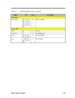
M1521 Signal Descriptions
Signal
Pin
Type
Description
Host Interface
A[31:29]
A[28:26]
A[25:23]
A[22:20]
A[19:17]
A[16:14]
A[13:11]
A[10:08]
A[07:05]
A[04:03]
W8, W11, U11, Y10,
Y9, V10, W9, W10, U9,
U10, V9, U5, V5, W5,
Y5, U6, W6, V6, Y6,
U7, W7, Y7, V7, V8,
Y8, Y12, U8, Y11, V11
I/O
Host Address Bus Lines. A[31:3] have two
functions. As inputs, along with the byte enable
signals, these serve as the address lines of the host
address bus that defines the physical area of
memory or I/O being accessed. As outputs, the
M1521 drives them during inquiry cycles on behalf of
PCI masters.
BEJ[7:0]
M1, L4, L3, L2, L1, K4,
K3, K2
I
Byte Enables. These are the byte enable signals for
the data bus. BEJ[7] applies to the most significant
byte and BEJ[0] applies to the least significant byte.
They determine which byte of data must be written to
the memory, or are requested by the CPU. In local
memory read and line-fill cycles, these are ignored
by the M1521.
ADSJ
T5
I
Address Strobe. The CPU or M1521 starts a new
cycle by asserting ADSJ first. The M1521 does not
precede to execute a cycle until it detects ADSJ
active.
BRDYJ
M5
O
Burst Ready. The assertion of BRDYJ means the
current transaction is complete. The CPU
terminates the cycle by receiving 1 or 4 active
BRDYJs depending on different types of cycles.
NAJ
N5
O
Next Address. It is asserted by the M1521 to inform
the CPU that pipelined cycles are ready for
execution.
AHOLD
L5
O
CPU A-Hold Request Output. It serves as the input
of CPU's AHOLD pin and actively driven for inquiry
cycles.
EADSJ
R5
O
External Address Strobe. This signal is connected to
the CPU EADSJ pin. During PCI cycles, the M1521
asserts this signal to proceed snooping.
BOFFJ
P5
O
CPU Back-Off. If BOFFJ is sampled active, CPU
floats all its buses in the next clock.
HITMJ
T8
I
Host Cache Hit after Modified. When snooped, the
CPU asserts HITMJ to indicate that a hit to a
modified line in the data cache occurred. It is used
to prohibit another bus master from accessing the
data of this modified line in the memory until the line
is completely written-back.
Summary of Contents for AcerNote Light 370P
Page 6: ...vi ...
Page 26: ...1 8 Service Guide Figure 1 5 Main Board Layout Bottom Side ...
Page 49: ...System Introduction 1 31 1 5 1 3 Power Management Figure 1 14 Power Management Block Diagram ...
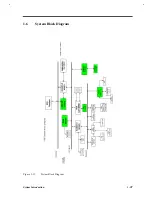
Page 55: ...System Introduction 1 37 1 6 System Block Diagram Figure 1 15 System Block Diagram ...
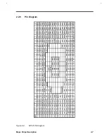
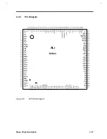
Page 64: ...Major Chips Description 2 7 2 2 5 Pin Diagram Figure 2 4 M1521 Pin Diagram ...
Page 99: ...2 42 Service Guide 2 5 3 Pin Diagram Figure 2 10 C T 65550 Pin Diagram ...
Page 117: ...2 60 Service Guide Figure 2 12 Functional block diagram CardBus Card Interface ...
Page 119: ...2 62 Service Guide Figure 2 14 PCI to CardBus terminal assignments ...
Page 135: ...2 78 Service Guide 2 7 3 Pin Diagram Figure 2 16 NS87336VJG Pin Diagram ...
Page 145: ...2 88 Service Guide 2 8 2 Pin Diagram Figure 2 17 YMF715 Block Diagram ...
Page 185: ...Disassembly and Unit Replacement 4 5 Figure 4 3 Disassembly Sequence Flowchart ...
Page 209: ...B 2 Service Guide ...
Page 210: ...Exploded View Diagram B 3 ...

