2-10
Service Guide
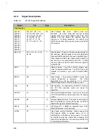
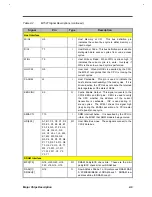
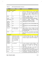
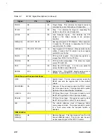
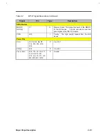
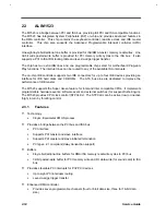
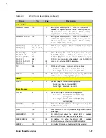
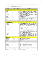
Table 2-2
M1521 Signal Descriptions (continued)
Signal
Pin
Type
Description
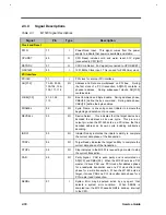
DRAM Interface
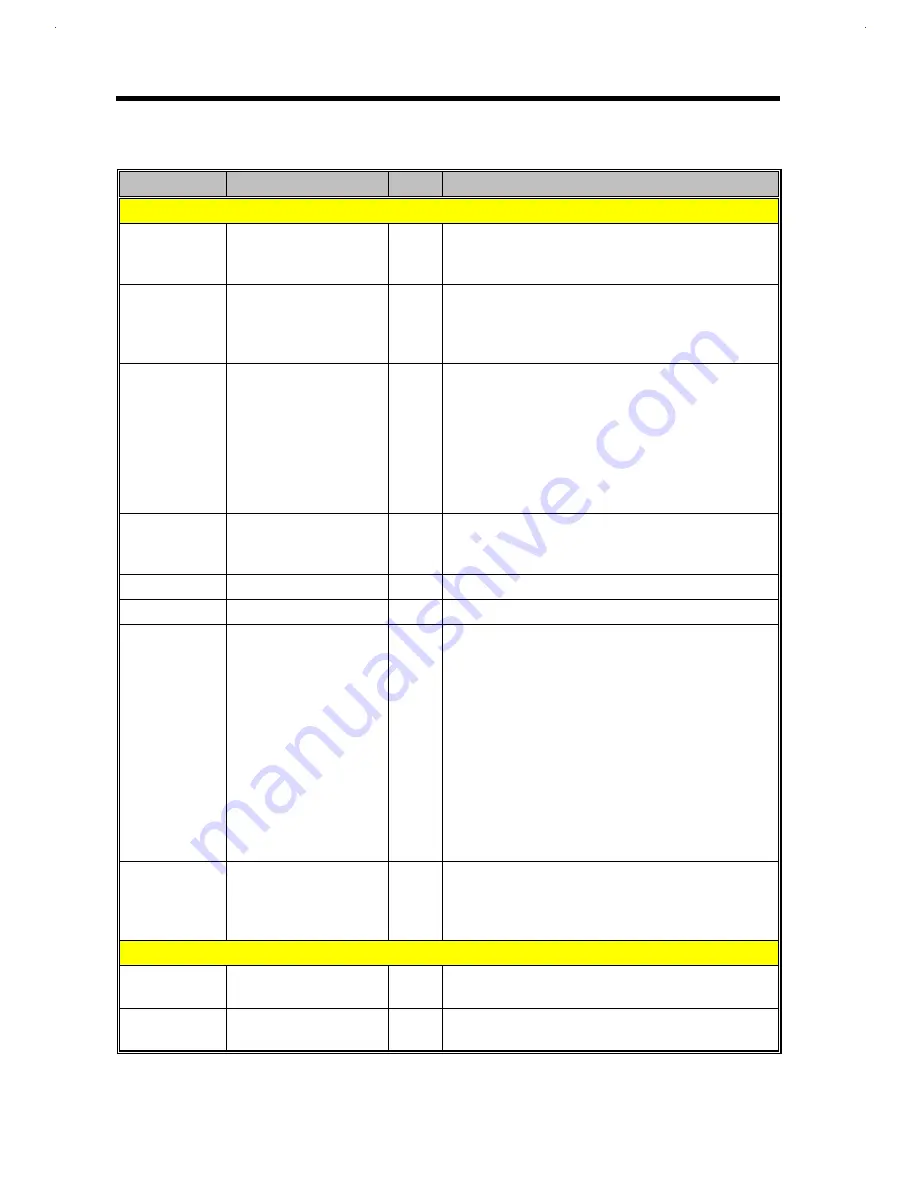
RASJ[6] /
SCASJ[0]
M16
O
Row Address Strobe 6, or Synchronous DRAM CAS
0 (FPM/EDO/BEDO) of DRAM bank 6. SDRAM
column address strobe (SDRAM) copy 0.
RASJ[5:0] /
SCSJ[5:0]
N17, M17, E16, F16,
F17, G17
I/O
Row Address Strobes or synchronous DRAM chip
select. These signals drives the corresponding
RASJs of DRAMs or synchronous DRAM chip
select[5:0].
CASJ[7:0] /
DQM[7:0]
L16, G16, J16, H16,
L17, H17, K17, J17
O
Column Address Strobes or Synchronous DRAM
Input/Output Data Mask. These CAS signals should
connect to the corresponding CASJs of each bank of
DRAM. The value of CASJs equals that of HBEJs
for write cycles. During DRAM read cycles, all the
CASJs are active. In SDRAM, these pins act as
synchronized output enables during a read cycle and
a byte mask during a write cycle.
MA[11:2]
V14, Y14, Y15, U14,
W14, T13, U13, V13,
W13, Y13
O
DRAM Address lines. These signals are the address
lines of all DRAMs. The M1521 supports DRAM
types ranging from 256K to 64M.
MAA[1:0]
T12, V12
O
Memory Address copy A for [1:0]
MAB[1:0]
U12, W12
O
Memory Address copy B for [1:0]
MD[63:0]
C15, A16, B17, A18,
B19, B20, D19, E20,
J19, K20, M18, N19,
P20, R19, T18, V20,
C14, D15, C16, D17,
A20, C20, E18, F19,
K18, L19, M20, P18,
R17, T20, U19, V19,
B14, D16, A17, C17,
A19, D18, E17, E19,
J20, L18, M19, N20,
P17, R18, U20, U18,
C13, B15, B16, B18,
C18, C19, C20, F18,
K19, L20, N18, P19,
R20, T19, T17, W20
I/O
Memory Data. These pins connect to DRAMs.
MWEJ[0]
T11
O
DRAM Write Enable. This is the DRAM write enable
pin and behaves according to the early-write
mechanism; i.e. it activates before the CASJs do.
For refresh cycles, it remains deasserted.
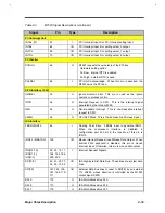
Secondary Cache Interface
CADVJ/CA4
V15
O
Synchronous SRAM advance or Asynchronous
SRAM address line 4.
CADSJ/CA3
W15
O
Synchronous SRAM address strobe cache or
Asynchronous SRAM address line 3.
Summary of Contents for AcerNote Light 370P
Page 6: ...vi ...
Page 26: ...1 8 Service Guide Figure 1 5 Main Board Layout Bottom Side ...
Page 49: ...System Introduction 1 31 1 5 1 3 Power Management Figure 1 14 Power Management Block Diagram ...
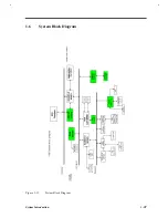
Page 55: ...System Introduction 1 37 1 6 System Block Diagram Figure 1 15 System Block Diagram ...
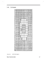
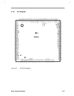
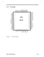
Page 64: ...Major Chips Description 2 7 2 2 5 Pin Diagram Figure 2 4 M1521 Pin Diagram ...
Page 99: ...2 42 Service Guide 2 5 3 Pin Diagram Figure 2 10 C T 65550 Pin Diagram ...
Page 117: ...2 60 Service Guide Figure 2 12 Functional block diagram CardBus Card Interface ...
Page 119: ...2 62 Service Guide Figure 2 14 PCI to CardBus terminal assignments ...
Page 135: ...2 78 Service Guide 2 7 3 Pin Diagram Figure 2 16 NS87336VJG Pin Diagram ...
Page 145: ...2 88 Service Guide 2 8 2 Pin Diagram Figure 2 17 YMF715 Block Diagram ...
Page 185: ...Disassembly and Unit Replacement 4 5 Figure 4 3 Disassembly Sequence Flowchart ...
Page 209: ...B 2 Service Guide ...
Page 210: ...Exploded View Diagram B 3 ...

